With the rapid pace of innovation and change at SK hynix, days quickly turn into weeks and weeks into years – and before you know it, 10 years have passed in the blink of an eye. The company, the industry, and even the world, have come a long way in these past 10 years — the growth and advancement of each one related to the other. Collectively, the impact has been huge.
Speeding towards the future of innovation, teams at SK hynix are often focused on the years to come – rather than on those that have passed. It is milestone moments like the end of a decade that offer us a unique opportunity to pause and reflect on our accomplishments and achievements.
As the decade draws to a close, SK hynix takes a look back at the 10 breakthrough moments in chronological order that defined it – and that will continue to define our future.

1. Full-scale mass production of 16nm NAND flash(November 2013)
In order to actively respond to the needs of its customers, SK hynix started the full-scale mass production of 16nm 64Gb (Gigabit) MLC (Multi Level Cell) NAND Flash. This innovation brought the industry’s thinnest process technology and was more cost competitive due to its smaller chip size. The announcement began SK hynix’s reputation to bring forth a competitive NAND portfolio with high reliability and endurance.
2. Development of the world’s first next-generation mobile memory LPDDR4(December 2013)
At the end on 2013, SK hynix took large steps to heighten its technology leadership by developing the world’s first 8Gb LPDDR4 product with 20nm-class technology. LPDDR4 was the next generation mobile DRAM interface, which was on the process of standardization at that time, and gave customers ultrahigh speed and low power consumption. In fact, the product ran two times faster and does so at lower voltage than of its existing LPDDR3.
3. Development of the world’s first, highest density 128GB DDR4 module(April 2014)
SK hynix made a significant advancement in the ultrahigh density server market with the announcement that it had developed the world’s first and highest density of 128GB (Gigabytes) module based on 8Gb DDR4 using its advanced 20nm-class technology. This module has double density compared to the company’s existing 64GB by taking advantage of TSV (Through Silicon Via) technology. This product helped cement the company’s reputation on providing premium DRAM with high density, ultrahigh speed, and low power consumption.
4. Development of the world’s highest density 16GB NVDIMM(October 2014)
In late 2014, SK hynix announced that it had developed the world’s highest density 16GB NVDIMM (Non-Volatile DIMM) based on 4Gb DDR4 using its advanced 20nm-class technology. By combining DRAM, NAND Flash and the controller in a single module, this product was able to send DRAM data to NAND Flash, whose density was two times bigger than the DRAM, in an unanticipated power loss, thus saving and restoring data safely. Ahead of mass production, SK hynix provided samples to several customers and the product got attention from corporations developing servers and operating systems in need of higher stability.
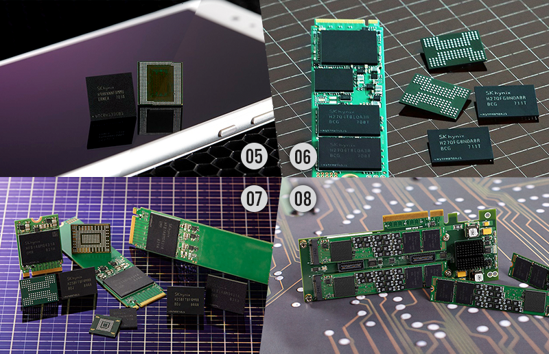
5. Launch of the world’s first, highest density 8GB LPDDR4X(January 2017)
SK hynix launched 8GB LPDDR4X mobile DRAM, the world’s highest density in the LPDDR4X standard, using its state-of-the-art dual channel 16Gb chips aimed to suit the upcoming flagship smartphone lineups. This technology allowed mobile device users to maximize their experiences and was expected to be included in various applications such as high-end laptops and automotive electronics.
6. Introduction of the world’s highest 72-layer 3D NAND Flash(April 2017)
In 2017, SK hynix unveiled the industry’s first 72-Layer 256Gb 3D NAND Flash based on its TLC (Triple-Level Cell) arrays and own technologies. This innovation stacked 1.5 times more layers than the already widely available 48-Layer 3D NAND, achieving 30% more productivity. 3D NAND is widely used in AI (Artificial Intelligence), big data and cloud storage. With this achievement, SK hynix secured the industry’s finest 3D NAND product portfolio, solidifying its business competence in NAND memory solutions.
7. Launch of the world’s first “CTF-based 96-layer 4D NAND Flash”(November 2018)
SK hynix was the first in the industry to combine the 3D CTF (Charge Trap Flash) design with PUC (Peri. Under Cell) technology. This 96-Layer 512Gb “CTF-based 4D NAND Flash” based on its TLC arrays reduced more than 30% of chip size and increased bit productivity per wafer by 49% compared to the company’s 72-layer 512Gb 3D NAND. It also provided a 30% higher write and 25% higher read performance. This achievement marks a milestone for the company’s NAND Flash business as a platform for developing future products.
8. Demo of the industry’s first ZNS-based SSD solution for data centers(March 2019)
SK hynix began 2019 with a strong first quarter when the company demonstrated the industry’s first ZNS (Zoned Namespaces) SSD solution at the 2019 OCP Global Summit in San Jose, CA. The ZNS SSD boasted 30% improvement in speed and reliability compared to the existing SSD, as well as more than four
times longer lifetime, making it suitable for the next-gen data centers. SK hynix plans to launch commercial products in the first half of 2020.
9. Mass production of the world’s first 128-layer 4D NAND(June 2019)
In another major milestone this year, SK hynix started mass-producing world’s first 128-Layer 1Tb (Terabit) TLC NAND, the highest vertical stacking and highest density for a TLC NAND Flash chip. This feat was accomplished only eight months after the company previously announced the 96-Layer 4D NAND last year. The new NAND Flash chip has significantly improved profitability with 40% higher productivity and 60% better investment efficiency, targeting high-capacity mobile and enterprise SSD customers.
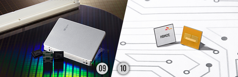
10. Development of the world’s fastest High Bandwidth Memory, HBM2E(August 2019)
Earlier this year, SK hynix developed the world’s fastest high bandwidth memory, HBM2E. As the DRAM technology here supports 460GB per second (3.6Gbps per Pin) data processing speed performance, the product is expected to be adopted by high-end machine learning, supercomputers and artificial intelligence. The new HBM2E boasts approximately 50% higher bandwidth and 100% additional capacity compared to the previous HBM2. It will strengthen SK hynix’s leadership in the premium DRAM market.
If we had to sum up the progress of the memory industry – and the continued improvement of SK hynix’ products – over the past 10 years, we would say: smaller, better, faster. From 2013’s mass production of the 16nm NAND flash to 2017’s introduction of the world’s highest 72-layer 3D NAND Flash, to 2019’s development of the world’s fastest HBM2E, we’ve delivered reduced chip sizes, ultrahigh speeds, and higher-quality experiences to our clients around the world.
While no one knows for certain what the next decade will bring, we certainly can say that the innovations of SK hynix will be at its core.


