An introduction to Inline Re-distribution Layer (IRDL) and its key features
The demand for mobile memory is steadily enhancing along with the consistent growth of mobile and wearable devices. When it comes to mobile devices, portability is pretty much everything which is why low-power and ultra-thin PKG technology has established itself as an essential element for the semiconductor industry.
Inline Re-distribution Layer (IRDL) technology is an advanced FAB technology that forms wiring by using an extra metal layer with an insulation layer and aluminum, enabling IO pads to relocate freely to the PKG wire bonding position where necessary. This technology allows you to make chip-to-chip bonding thinner and simpler. Additionally, IRDL, one of RDL technologies, was named so as the entire process takes place inside a FAB, unlike PKG RDL.
The figures below show the two MCP1 methods for chips. “Vertical-Stack MCP” (left) is the existing technique where upper chips stack vertically on the lower chips’ bonding pad. “Shift-Stack MCP using RDL,” (right) on the other hand uses a shift-stacked method by avoiding the bonding pad. This way, wire interference and short from wire to chip that could occur within the vertical-stack MCP can be prevented. The gap between the upper chip and the lower chip reduces when this new method is applied, making it significantly easier to meet the proper thickness that the customers require.
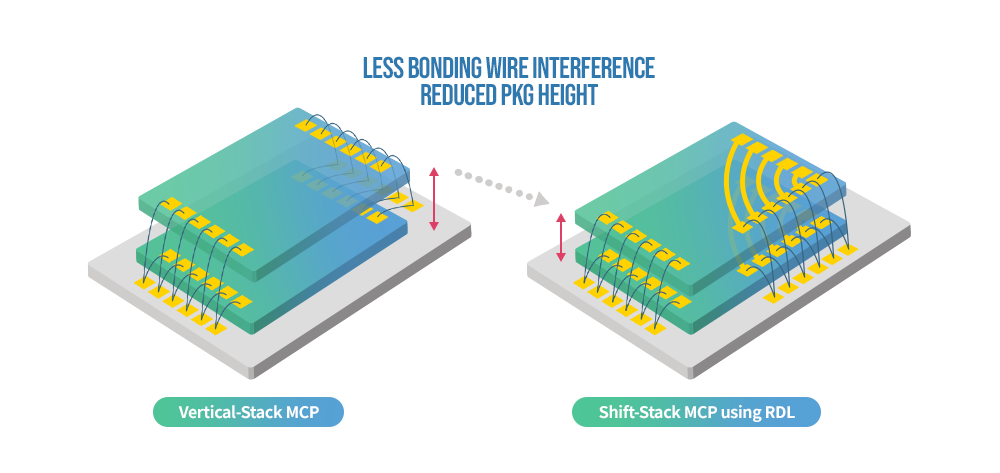
Figure 1. Vertical-Stack MCP vs Shift-Stack MCP

Figure 2. Cross-Sectional View of Figure 1
Comparing existing PKG RDL and IRDL processes
The major difference between PKG RDL and IRDL lies within the structure formation method, so let’s learn more about the benefits of IRDL.
PKG RDL’s structure formation method is largely divided into two processes: FAB-in and FAB-out. The FAB-in process involves covering a top metal by an insulating material with only pads open. Then, in the FAB-out process, you apply the 1st dielectric layer to separate the RDL line from the insulating materials on top of the wafer, and form lines using gold. After that, a 2nd dielectric layer is applied to cover the top of the line.
On the other hand, in the IRDL method, you use the insulating materials to cover the top metal and form VIA to open the pads. Then, you use aluminum to form lines, which is different from PKG RDL. Afterward, you apply insulating materials on top.
IRDL has the same purpose to relocate pads as PKG RDL. However, IRDL holds three major strengths courtesy of the RDL as the process progresses inside the FAB:
• Firstly, net die improves since circuits can be located under the pads.
• Secondly, the use of aluminum instead of gold lowers the cost of the entire process by up to 30%.
• Lastly, a chip’s performance is enhanced since circuit designer can utilize RDL for strengthening power mesh2.

Figure 3. Comparing PKG RDL with IRDL
Smaller chips better net die with circuits placed under the pad
When using the existing PKG RDL structure, numerous issues relating to the pad would often occur during probing and bonding, as the metal on top was too thin – under 1um level.
With the IRDL structure, it allows the thickness of the top metal almost 10um level enough to endure the stress generated during the probing and bonding, which allows placing the circuit under the pad. As a result, it can improve net die by reducing the chip’s size.
Reinforce PDN with IRDL
A reinforced power mesh using IRDL leads to power distribution network (PDN) enhancement, resulting in a much-improved chip performance. Without IRDL, PDN reinforcement can only be done with the chip’s existing metal wiring, causing PDN deterioration in far area from the pad. Reinforcement was therefore very limited with this method. On the other hand, when using IRDL, the freedom of reinforcement was greatly increased as it delivers a lower resistance value due to the nature of the RDL layer. Therefore, the performance of a chip can be improved by using IRDL.
IRDL: A Precursor for future devices
IRDL technology achieved a low-cost process with accomplishment on its main purpose of relocating IO pads to a position where PKG requires, without compromising an existing chip’s architecture. It has already made big contributions to SK hynix’s leading technologies in the mobile market, by decreasing the thickness of finished products. It allows the company to match the future direction of mobile devices – thinner products. Securing this element technology is crucial for the industry as a whole, as it advances net die by reducing its size and strengthens the performance.
1MCP: Multi Chip Package, a technology that stacks more than two semiconductor chips into a single package to increase capacity and performance while reducing its mounting space – used predominantly for slim portable devices such as smartphones and tablet PCs. Thinner chips can be made during MCP using IRDL technology.
2Power mesh: A network that consists of power lines on multiple metal layers.

BySeonsoon Kim
Head of DRAM PI at SK hynix Inc.


