Fact Sheet
SK hynix Inc., headquartered in Korea, is the world’s top tier semiconductor supplier offering Dynamic Random Access Memory chips (“DRAM”), Flash memory chips (“NAND Flash”) and CMOS Image Sensors (“CIS”) for a wide range of distinguished customers globally.
At A Glance


Products & Services
Sales Breakdown (as of 2023, Korea)

Business Areas

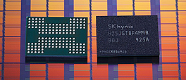
DRAM
Aiming to lead the global DRAM industry by providing high-quality DRAM products for diverse needs and markets, including mobile and server, through innovative technology development.
NAND
Manufacturing the latest NAND flash such as TLC and QLC, while continuously developing products with higher data processing speed and a wide range of capacities.
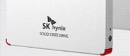
SSD
Also providing the best NAND Flash solutions to meet the diverse needs of the customers, particularly with revolutionary high-quality SSDs for enterprise, clients, and consumers.

CIS
Planning to lead a new chapter in CIS market through high-resolution CMOS sensors serving as a electronic eyes.
Employees

46,255
Number of
Employees
As of 2023

7,574
(16%)
Global Employees
Excluding Korea

34.1%
Ratio of
Female Employees
Brand Identity


SK hynix is ushering in a new future by leading the technology-based IT ecosystem. With a tenacious commitment and technological innovations, SK hynix is striving to make a future where all stakeholders and members of society enjoy shared growth. By establishing a system with a new brand identity, SK hynix is aiming to become a maker of a better world that is at the core of advanced technology.
Double Bottom Line

SK hynix recognizes social responsibility as an integral part of gaining the trust of our stakeholders and taking our corporate value to the next level. We have already declared the Double Bottom Line (DBL) Management System in pursuit of both economic and social value creation and have taken initiatives to balance these two values while gaining competitive advantages. With SK Management System’s (SKMS) philosophy that “All value that a company creates for the happiness of its stakeholders is social value” and that by creating social value a company “will elevate its economic value and develop a relationship of trust with its stakeholders,” SK hynix has expanded the meaning of social value to include the pursuit of employees’ happiness and resolving social issues.
Sustainability Report
Business History
- 2023
- 2022
- 2021
- 2020
- 2019
- 2018
- 2017
- 2016
- 2015
- 2014
- 2013
- 2012
- 2011
- 2010
- 2009
- 2008
- 2007
- 2006
- 2005
- 2004
- 2003
- 2002
- 2001
- 2000
- 1999
- 1998
- 1997
- 1996
- 1995
- 1994
- 1993
- 1992
- 1991
- 1990
- 1989
- 1988
- 1987
- 1986
- 1985
- 1984
- 1983
2023
- Aug Developed HBM3E with the world’s best specifications
Developed LPDDR5X DRAM with the world’s highest capacity
Unveiled samples of the world’s tallest NAND with 321 layers - Jun Initiated mass production of the world’s tallest 4D NAND with 238 layers
- Apr Developed the world’s first 12-layer HBM3
- Jan Developed the world’s fastest mobile DRAM, LPDDR5T
2022
- Sep Announced plans to build the M15X plant
- Aug Completed the acquisition of a key foundry
Developed the world’s tallest NAND with 238 layers - Jun Started mass production of HBM3 DRAM
- Mar Appointed Kwak Noh-Jung as president and CEO
10th anniversary of the company’s incorporation into SK Group - Feb Developed next-generation semiconductor memory, PIM
- Jan Launched ICT alliance with SK Telecom and SK Square
2021
- Dec Closed the first deal in the acquisition of Intel’s NAND business
- Oct Developed the world’s first HBM3 DRAM
- Jul Full-scale mass production of 10nm class 4th-gen DRAM using EUV
- May Announced 2020 social value (SV) achievements
- Mar Started mass-production of LPDDR5 Mobile DRAM with industry’s largest capacity
Board appointed Park Jung-ho as Co-CEO - Feb Announced the completion of M16 Plant construction
- Jan Announced SV 2030, a roadmap for maximizing social values
2020
- Dec Joined RE100 (Renewable Energy 100)
Unveiled the industry’s most multilayered 176-layer 4D NAND flash - Oct Launched world’s first DDR5 DRAM
Announced to acquire Intel NAND memory business - Sep Invested in AI specialized company ‘Gauss Labs Inc.’ to lead SK’s future value creation
- Aug Launched Gold P31, the world’s first 128-layer NAND consumer PCIe NVMe SSD
- Jul Started mass-production of high-speed DRAM, “HBM2E”
- Apr Won the grand prize of Water Security 2019 awarded by CDP
Started to sample “PE8000” series, the company’s newest and most advanced line-up of eSSDs
2019
- Dec Received Environmental Product Declaration for 10nm-Class LPDDR4 Products
- Oct Developed 1Znm 16Gb DDR4 DRAM
- Aug Unveiled “Gold S31” Consumer Solid-State Drive on Amazon
Developed the industry’s fastest HBM2E - Jun Started mass-producing the world’s first 128-layer 1Tb TLC 4D NAND
- May Shipped samples of 96-layer 1Tb QLC 4D NAND
- Apr Completed expanded fab (C2F) in Wuxi, China
- Mar Announced KRW 1.2 trillion support plans for mutual growth at the “Semiconductor Cluster”
Demonstrated industry’s first ZNS-based SSD solution for next-gen data centers - Feb A Special Purpose Company (SPC) submitted an Investment Letter of Intent for a “Semiconductor Cluster” to Yongin city government
2018
- Dec Broke ground for M16 at its headquarters in Icheon
Appointed Dr. Seok-hee Lee as the new Chief Executive Officer - Nov Developed 1Ynm 16Gb DDR5 DRAM
Developed 1Ynm 8Gb DDR4 DRAM
Launched the world’s first ‘96-layer CTF-based 4D NAND Flash’ - Oct Introduced a new slogan “We Do Technology”
Held a ceremony celebrating the completion of M15 in Cheongju - Jul Announced a construction plan of a new semiconductor fabrication plant in Icheon
- Jun Completed procedure to take over Toshiba Memory through consortium between Korea, America and Japan
- May Completion of Happy More, ‘Subsidiary Standard Workplace for People with Disabilities’
- Mar Introduction of outside director system and establishment of continuous management commission within the board of directors
- Feb Development of 4th generation (72 phase) 3D NAND-based 4TByte SATA SSD for business use
Started 4th generation (72 phase) NAND-based next generation PCIe eSSD customer certification
2017
- Oct Operated “SK hynix Industrial Health Advancement Continuation Committee”
- Sep Presented construction plan for the Icheon Campus Research and Development Center
Investment decision for Toshiba Memory - Jul Established ‘SK hynix System IC’, which is a subsidiary specializing in foundry
- Apr Introduced Industry’s Fastest 8Gb Graphics DRAM(GDDR6)
Introduced Industry’s Highest 72-Layer 3D NAND Flash - Jan Launched the World’s First Highest Density of 8GB LPDDR4X
2016
- Dec Announced construction of a cutting-edge NAND Flash FAB in Cheongju
- Oct Entered into an agreement with Stanford University to R&D ‘Artificial Neural Network Devices’
Joined the nation’s first ‘Platinum Club’ of CDP’s the best honor - Aug MOU for an establishment of ‘Subsidiary Typed Standard Workplace’ with KEAD
- Feb Launched a handball team ‘SK Hawks’
2015
- Aug Established M14 line in Icheon
Expanded IP and commercial relationship with SanDisk - Jun Introduced industry’s first model of wage sharing with business partners
- Feb the world’s first commercialization of 8Gb LPDDR4
- Jan Announced all-time high financial results for FY2014
2014
- Dec Signed a MOU for joint development of nano imprint lithography with Toshiba
- Oct Developed the world’s first 16GB NVDIMM
- Sep Established a back-end line in Chongqing, Sichuan Province, China
Listed on the DJSI World for 5 consecutive years
Developed the world’s first wide IO2 mobile DRAM - Jun Acquired firmware division of Softeq Development FLLC.
- May Acquired PCIe card division of Violin Memory
- Apr Developed the world’s first 128GB DDR4 module
2013
- Dec Developed the world’s first 20nm class LPDDR4
Developed the world’s first TSV-based HBM - Nov Established mass production system of 16nm NAND flash
- Oct Developed the world’s first 20nm Class 6Gb LPDDR3
- Aug Opened an integrated analysis center
- Jul Signed a cross license agreement with Samsung Electronics Co.
- Jun Signed a patent license agreement with Rambus
Developed the world’s first high density 8Gb LPDDR3 - Feb Appointed Dr. Sung Wook Park as the new chief executive officer
2012
- Sep Developed low-voltage 4Gb graphics DDR3
Launched the flash solution design center - Jun Established M12 line in Cheongju
Launched client-side SSD
Acquired Link_A_Media devices
Acquired Ideaflash S.r.l. and established a flash R&D center in Europe
Signed joint development for PCRAM with IBM - Apr Signed a strategic alliance with Spansion
- Mar Changed the company name to ‘SK hynix Inc.’
- Feb SK Telecom becomes Hynix’s largest shareholder
Appointed Mr. Tae-won Chey as the new chairman & chief executive office
Appointed Mr. Sung Min Ha as the chairman of board of directors
2011
- Nov SK Telecom signed the share purchase agreement with the Hynix share management council
- Jul Signed joint development for MRAM with Toshiba
- Jun Appointed Mr. In-Baik Jeon as the chairman of BOD
- Apr Developed 30nm-class 2Gb high performance DDR4 DRAM
- Mar Developed 40nm-class 16Gb DDR3 DRAM using TSV technology
2010
- Sep Named to Dow Jones sustainability world index
Signed a joint development agreement with HP on Next Generation Memory Products, ReRAM - Jun Completed construction of a back-end joint venture, HITECH semiconductor package & test, in China
- Mar Appointed Mr. Oh Chul Kwon as the new chief executive officer
- Feb Developed 20nm-class 64Gb NAND flash
- Jan Developed the world’s first 2Gb Mobile Low Power DDR2 DRAM
2009
- Dec Introduced the world’s first 40nm Class 2Gb GDDR5 DRAM
- Nov Acquired Intel validation for 40nm Class 2Gb DDR3 products
- Oct Introduced the second generation 1Gb DDR3
- Aug Introduced 4Gb mobile DDR SDRAM supported on Intel’s Moorestown platform
- May Announced the world’s first 8GB 2-Rank DDR3 R-DIMM validation
- Apr Developed the world’s first Low Power-High Speed Mobile 1Gb DDR2 DRAM
- Mar Announced the world’s first 8GB 2-Rank DDR3 R-DIMM validation
- Feb Developed the world’s first 44nm DDR3 DRAM
- Jan Acquired Intel validation for the world’s first ultra-high speed DDR3 based module for servers 4GB ECC UDIMM
2008
- Dec Developed the world’s first 2Gb Mobile DRAM
- Nov Introduced industry’s fastest 7Gbps, 1Gb GDDR5 graphics DRAM
- Aug Completed construction of 300mm fabrication plant of 3rd factory in Cheongju
US decided to lift countervailing duty order on DRAM
Demonstrated world’s first 16 GB 2-Rank R-DIMM using metaRAM™ technology
Numonyx and Hynix extend efforts to introduce new, innovative NAND flash memory products and technologies - Jul Announced closure of Eugene fabrication plant
- May Signed amendment to strengthen long-term strategic alliance with ProMOS
- Apr Released the ‘Sustainability Report’
Applauded the council of the European Unions move to lift countervailing duties on Hynix DRAMs
Developed the world’s fastest Mobile LPDDR2
Signed license and joint development agreement on Spin-Transfer Torque MRAM (STT-RAM) with Grandis - Mar Announced new board of directors
Contracted with Fidelix for strategic alliance - Feb Introduced 2-Rank 8GB DDR2 RDIMM
Announced strengthening R&D sector - Jan Signed an agreement for cooperating joint R&D program of next-generation non-volatile memory technology
Arranged Toyota benchmarking program in order to establish innovative system
Announced 800MHz, 1GB/2GB UDIMM validation
Held a strategic management workshop for sustainability managementt
2007
- Dec Successfully offer global convertible notes
Opened a new webpage - Nov WTO upholded ruling against Japan over punitive tariffs on imports of Hynix chips
Signed on CIS business cooperation with SiliconFile
Introduced ‘New Working Board System’
Acquired Intel validation for 1Gb DDR2 DRAM
Developed industry’s first 1Gb GDDR5 DRAM - Oct Signed an agreement for cooperating environmental management with Korean Federation for Environmental Movement
Signed technology and licensing agreement for PRAM with Ovonyx - Sep Hynix-ST Semiconductor Ltd. Signed to Sell 200mm equipment to CRH
Developed the world’s first NAND Flash MCP with 24 stacked chips - Aug Reached license agreement with ISi on Z-RAM memory technology
Developed industry’s fastest, smallest 1Gb mobile DRAM - Jul Announced corporate slogan ‘Good Memory’
Announced corporate mid-long term master plan - May Developed the world’s first NAND Flash 24 stacks multi chip package
Acquired the industry’s first validation on DDR3 DRAMs from Intel - Apr Achieved the top-level operating profit margin
Launched mass production of DOC H3 - Mar Appointed Mr. Jong-Kap Kim as the new chairman & CEO
Reached patent cross license agreement and signed MOU to form joint venture for x4 technology with SanDisk
Signed semiconductor patent cross licensing and supply agreements with Toshiba
Announced ‘ECO Mark’
Developed the world’s fastest ECC mobile DRAM
Announced new board of directors - Jan Posted record revenue and profit for 2006
Developed the fastest memory module based on ‘Wafer Level Package’ technology
2006
- Dec Announced industry’s first 60nm 1Gb DDR2 800MHz based modules
Developed the world’s fastest 200MHz 512Mb mobile DRAM - Oct Posted record high revenues since foundation
Established a global manufacturing network with complete construction of Hynix-ST Semiconductor Inc - Sep Launched 300mm research fab line
- Mar Acquired the industry’s first validation on 80nm 512Mb DDR2 DRAMs from Intel
- Jan Announced joint development plan of DOC H3 (new generation DiskOnChip embedded flash drive) with M-Systems
2005
- Dec Developed the world’s first 512Mb GDDR4, the industry’s fastest and highest density graphics DRAM
- Nov Launched the industry’s first JEDEC standard 8GB DDR2 R-DIMM
- Jul Received industry’s first Intel validation on high density-high speed 2GB DDR2-667 SODIMMs
Emerged from Corporate Restructuring Promotion Act ahead of schedule - Jun Completed successful fund-raising of $1.8 billion through overseas bond issue and syndicated loan in local market
Developed industry’s first ultra-high-speed DDR2-800 memory module and received validation from Taiwan-based ASUS - May Began mass production of chips from 12-inch plant, M10
- Apr Launched Hynix-ST joint venture construction in Wuxi City, Jiangsu Province, China
- Mar Posted record high operating profit for year 2004 as a whole
- Jan Developed x8-based memory modules for servers with 30 pct higher power efficiency
Contracted with Taiwan-based ProMOS for strategic alliance
Signed strategic alliance contract with Taiwan’s ProMOS Technologies
2004
- Nov Signed contract with STMicroelectronics for setting up plant in China
- Oct Completed sale of non-memory business
- Aug Signed contract with Wuxi City government for setting up plant in China
- Jun Signed non-memory Business Transfer Agreement with System Semiconductor
- Feb Developed 512Mb NAND flash memory
Acquired DDR2 SDRAM validation From Intel
2003
- Dec Acquired 512Mb DDR2 SDRAM validation from Intel
- Sep Received fourth consecutive year Partners in Performance award from Selestica
- Aug Developed 0.18-micron high voltage process technology
Developed 1Gb DDR2 RAM - Jul Produced ultra-speed 256Mb DDR500
- Jun Acquired 512Mb DDR400 validation from Intel
Produced organic EL driver capable of lighting in 4,096 colors
Established research lab for environment, safety and technology - May Started mass production of ultra-low power 256Mb SDRAM for mobile phone use
Succeeded in mass production of 0.10-micron “Golden Chip” - Apr Strategically cooperated with STMicroelectronics in flash memory development
- Mar Developed commercialization technology of Fe RAM
Produced CMOS high-frequency PLL IC chip - Feb Acquired 256Mb DDR 400 validation from Intel
- Jan Acquired 333Mbps ultra-speed 512Mb DDR SDRAM validation from Intel Spun off HYDIS (TFT-LCD)
2002
- Sep Signed MOU to spin off Hydis
- Aug Developed the world’s first high-density, wide-bandwidth 256MB DDR SDRAM
Opened local website for memory module sale - Jul Developed bluetooth ‘Embedded Flash Base-Band Chip’
- Jun Developed the world’s first 256MB SDR SDRAM for high-end consumer application
- May Signed long-term agreement for foundry supply with Cirrus
- Mar Developed 1Gb DDR DRAM module
- Feb Acquired validation for DDR SDRAM from VIA
- Jan Signed agreement to transfer stake in “Hyundai Syscomm”
2001
- Dec Developed the world’s fastest 128Mb DDR SDRAM
Developed 8bit MCUs for car audio use and started mass production - Sep Sold TFT-LCD assets for $650m
- Aug Completed separation from Hyundai Group
- Jul Spun off CDMA Mobile Communication Equipment Manufacture Unit to ‘Hyundai Syscomm’
Launched mass production of MCU for flash memory cards - Jun Spun off Hynix’s Management Supporting Unit to “ASTEC”
Entered “Multi Chip Package” market
Developed two types of 32Mb super-low power flash memory - May Spun off Network Business Unit to ‘Hyundai Networks’
Completed official spin-off of ADSL operation
Developed 1Mb FeRAM
Completed official spin-off of handset operation to Hyundai CuriTel - Apr Started mass production of the world’s fastest DDR SDRAM for graphics
Introduced new CI
Acquired 288Mb RDRAM validation from Rambus - Mar Started to supply the world’s fastest DDR SDRAM module for main memory to Compaq Computer Corporation
Changed the Company name to ‘Hynix Semiconductor Inc.’
Developed 8Mb super-low power SRAM
Spun off Customer Service Operation to ‘Hyundai Digitech Service’ - Feb Sold Hyundai Electronics basketball team to KCC
Spun off Satellite Service Unit
Acquired validation from AMD and VIA for 128Mb and 256MB DDR SDRAM
Signed contract with Hewlett-Packard for exclusive memory module supply - Jan Received certificate on health and safety category from British Standards Institution
Developed Korea’s first Pb-free semiconductor
2000
- Dec Acquired Telecommunications Leadership 9000 certification Developed 256MB micro-semiconductor module
- Oct Launched collaborative product & process innovation system Entered India’s CDMA WLL equipment market Proclaimed new slogan as “Human & Digital”
- Sep Adopted corporate research commissioner system
- Aug Developed new 15.0/18.1 inch TFT-LCD module Launched satellite communications service for Asia-Pacific region Spun off Monitor Business Unit to “Hyundai Imagequest” Spun off PDP Business Unit
- Jul Strategically cooperated with LG Electronics in semiconductor business Received validation for electric money in China
Initiated global cash management system with Bank of America Started annual salary system - Jun Begun mass production of world-class 18.1-Inch TFT LCD monitor Launched new photoresist for semiconductors Entered Brazilian WLL terminal market
- May Acquired ISO 14001 from LRQA for environment-friendly management in all business units Exported ADSL system firstly in Korea
- Apr Sold Scotland’s semiconductor factory to Motorola
Succeeded in developing new Ferrolectric RAM, FeRAM Started production of ultra-low voltage flash memory Started mass production of MCU for recharging battery MPEG-4/7 technology was selected as international standard - Feb Received CMTL award from Intel at ‘Intel Developer Conference’
1999
- Dec Agreed on long-term supply contract of CDMA equipment with Airtouch
Implemented stock option system firstly among big Korean manufacturers - Nov 19 inch monitor was selected as best monitor by German PC magazine
- Oct Developed the world’s first new memory manufacturing process technology
Merged Hyundai Semiconductor Co,. Ltd. - Jul Took over large stockholder’s share of LG Semiconductor
- Jun Started mass production of the world’s fastest 16M synchronous DRAM for graphics
- May Agreed on stock transfer contract with LG Group and LG Semiconductor
- Mar Sold semiconductor assembly company (ChipPAC)
- Feb Produced Korea’s first MP3 decoder chip
1998
- Dec Succeeded in mass production of photosensitive material for 4G DRAM firstly in Korea and exported technology
Developed 0.25㎛ non-memory manufacturing technology - Nov Started mass production of the world’s fastest 128M SDRAM
- Oct Developed 4th generation 64M synchronous DRAM
- Sep Developed 64M DDR synchronous DRAM
Developed the world’s smallest direct RAMBUS DRAM
Developed next generation memory, FeRam - Aug MAXTOR (HDD manufacture and supply) IPO on NASDAQ
- Apr Marketed PCS with ‘Voice Recognition’ technology
- Mar MPEG-4 core technology was selected as international standard
- Feb Developed Korea’s first non-memory semiconductor for automobile
Self-developed Korea’s first 26 inch PDP
1997
- Dec Established 5 million-piece monthly production system of 64M DRAM chip
Developed Korea’s first digital HDTV broadcasting system - Nov Developed the world’s first Synclink DRAM test product
- May Developed the world’s first 1G synchronous DRAM using SOI technology
1996
- Dec Started IPO
- Oct Established semiconductor fab in Scotland, UK
- Sep Participated in Taiwan’s satellite communication service business
- Aug Participated in India’s satellite communication service business
- Feb Started construction of semiconductor plant in Oregon, USA (HSA)
- Jan Took over MAXTOR (HDD manufacture and supply)
1995
- Dec Entered best ten manufacturers in Korea
- Oct Developed the world’s first 256M SRAM
- Aug Established semiconductor plant in Oregon, USA (HSA)
- Apr Developed the world’s first MPEG-2 SAVI decoder chip
- Feb Established non-memory US corporation, SYMBIOS
1994
- May Established China corporation, HECS
- Apr Established US corporation, AXIL
- Mar Participated in GLOBALSTAR (artificial satellite business)
1993
- Dec Exceeded ten-million-set target line in car audio production
- Oct Signed technology agreement with FUJITSU
Exceeded 4 million-set target line in shipment of monitor
Acquired ISO 9002 on telecommunications category
Acquired ISO 9002 on car audio category firstly in Korea - Sep Acquired ISO 9001 on semiconductor category
- Aug Developed CD-VISION 2000
Developed car CD auto changer
Acquired ISO 9002 on computer category
Took over Maxtor (US HDD manufacturer)
Developed 1M Fast SRAM - Jul Acquired ISO 9002 on monitor & terminal category
Started pilot production of 16M DRAM in FAB IV - Jun Developed 8M MASK ROM
Completed construction of FAB IV
Developed HA, unmanned security system
Took over Gold Star’s camera assembly line - Mar Acquired ISO 9002 on hybrid IC & memory module category
Opened new Media Operation Division - Feb Developed GPS, automotive navigation apparatus for car thirdly in the world
- Jan Succeeded in developing and localizing Car CDP DECK
Developed IC card for memory extension
Developed 3 inch STN LCD
1992
- Dec Completed construction of FAB 2 B-Line
- Nov Was selected as the most excellent company by US Analog Devices-PMI in semiconductor assembly part
- Sep Developed 64M DRAM
Developed 64M DRAM sample product as government assignment
Acquired ISO 9002 in semiconductor assembly category
Developed 2nd generation 16M DRAM - Jul Developed DSP built-in car audio firstly in Korea
- Jun Operated automotive electronics division, IN-line System
- May Developed private switchboard HNT-832
- Mar Developed G4 FAX
- Jan Joo-yong Kim assumed office as CEO & president
1991
- Nov Developed 1M Slow SRAM
- Oct Domestically marketed the smallest and lightest mobile phone
- Aug Established Singapore corporation (HES)
Domestically marketed 486 PC - Jul Exceeded 1 hundred-million-piece target line in monthly semiconductor assembly capacity
- May Selected new CI for Hyundai Electronics
- Apr Started mass production of 4M DRAM
- Mar Developed 16M DRAM
- Feb Developed 16M DRAM pilot product as government assignment
1990
- Nov Exceeded 5 million-set target line in production of car audio
- Sep Started camera export to US
- Jul Held National S/W Competition for university students
- Apr Developed 1,200 bps PAGER firstly in Korea
- Feb Established HEA Semiconductor and Computer R&D Center
- Jan Started production of 1M DRAM
1989
- Nov Completed construction of FAB III Started production of VGA color monitor
- Oct Exported PC to Japan firstly in Korea
- Sep Exceeded 1 million-set target line in production of ARTPHONE and self-developed 4M DRAM
- Aug Developed 256K Fast SRAM
- Jul Produced 1 million sets of monitor
- May Formed Hyundai Electronics basketball team
- Apr Acquired top grade in Quality Control(Q.C) of car audio
Launched joint development of 16M DRAM - Jan Ranked 20th in the world semiconductor market
1988
- Dec Developed automatic answering phone
- Nov Developed automatic answering phone
- Oct Exceeded 2 million-set target line in car audio production Completed semiconductor assembly SMD line
- Jul Exceeded 7 million-piece mark in monthly sales
- Jun Developed 256K slow SRAM
Exceeded 500 thousand-set target line in export of monitor
Agreed on technical cooperation in ASIC with LSI Logics Co. in US - Apr Topped in export of PC in Korea
- Jan Completed development of 1M DRAM
1987
- Dec Car phone HKP-308 was selected as “Governmental Form Recognition No.1″
Started 3.5” FDD production - Oct Exceeded hundred- thousand-piece target line in export of car phone
Started export of 256K DRAM
Exceeded million-piece target line in export of car audio - Sep Developed 4th generation switchboard HX-400
- Aug Agreed on contract for 256K DRAM foundry supply with US-based TI
- Jul Agreed on technical cooperation in 256K SRAM with MOS Electronic Co.
- Apr Entered FA market
Launched satellite broadcasting receiver - Feb Topped in key phone sales
- Jan Agreed on OEM supply contract with AIWA in production of car audio
1986
- Nov Exceeded thousand-piece target line in production of “Hyundai Art phone”
- Oct Completed construction of FAB 1B- LINE
- Sep Developed 4M DRAM in joint with the government
- Aug Developed CMOS type 256K EPROM
- Jul Started OEM production of key phone
Developed private switchboard, PABXHX50 - Jun Held first employees’ culture fair, “Ami Carnival”
- May Started production and export of car audio CX-135E to Canada firstly in Korea
- Apr Opened semiconductor sales head office
Established semiconductor research institute - Mar Started production and sale of “ARTPHONE”
- Jan Opened software division head office
1985
- Dec Started shipment of 16K SRAM
- Oct Started mass production system of 256K DRAM
- Sep Started mass production of 400MHz key phone
- Jul Completed construction of semiconductor assembly plant
- May Marketed general phones in Korea
Started mass production of 16K SRAM
Started mass production of 64K DRAM - Apr Completed construction of car audio plant
- Mar Agreed on production and supply contract of semiconductor foundry with US-based TI
Started pilot production of semiconductor
1984
- Dec Succeeded in pilot production of 16K SRAM firstly in Korea
- Oct Opened US corporation, HEA
- Sep Completed construction of FAB II-A
- Aug Began construction of semiconductor assembly plant
- Apr Completed construction of communication equipment plant
Completed construction of information equipment plant - Feb Mong-hun Chung assumed office as CEO & president
1983
- Nov Started the first manufacturing of “Multifunctional Phone LX-2” as complete product
- Oct Began construction of Icheon plant
- May Agreed on contract of establishing PC sales agency with US-based IBM
- Mar Established US corporation (HEA)
- Feb Established Hyundai Electronics Co., Ltd
Began semiconductor business


