The semiconductor industry assumes a pivotal role in the AI era
The arrival of the AI era is not only reshaping the role of the semiconductor industry but also expanding the boundaries of the ecosystem itself. Often considered the backbone of the industry, semiconductors have long served as a foundational technology underpinning a wide range of industries and our everyday lives. As the AI era unfolds, semiconductors have now become the key driver of AI performance, offering a competitive service advantage and acting as a strategic infrastructure layer for the broader digital economy.
AI memory has become a focal point in this shift. Today, AI performance depends on far more than advances in algorithms alone. Even when running the same model, processing speed, cost, power efficiency, and user experience can vary significantly depending on the underlying computing architecture, memory system, and network architecture. This is one of the reasons HBM* has attracted so much attention in recent years. AI memory technologies such as HBM work alongside GPUs to deliver the data throughput required for AI workloads, making memory semiconductors a key determinant of AI performance. This reflects how the semiconductor industry is evolving beyond traditional manufacturing to become a critical foundation for the performance and scalability of the AI industry.
AI is no longer a competition defined solely by software or models. To deliver AI services in the real world, compute, memory, packaging, networking, and data center infrastructure must operate as an integrated system. Within this architecture, memory plays a much broader role than simple data storage, directly shaping AI performance and efficiency.
From a specialized supply chain to an integrated ecosystem
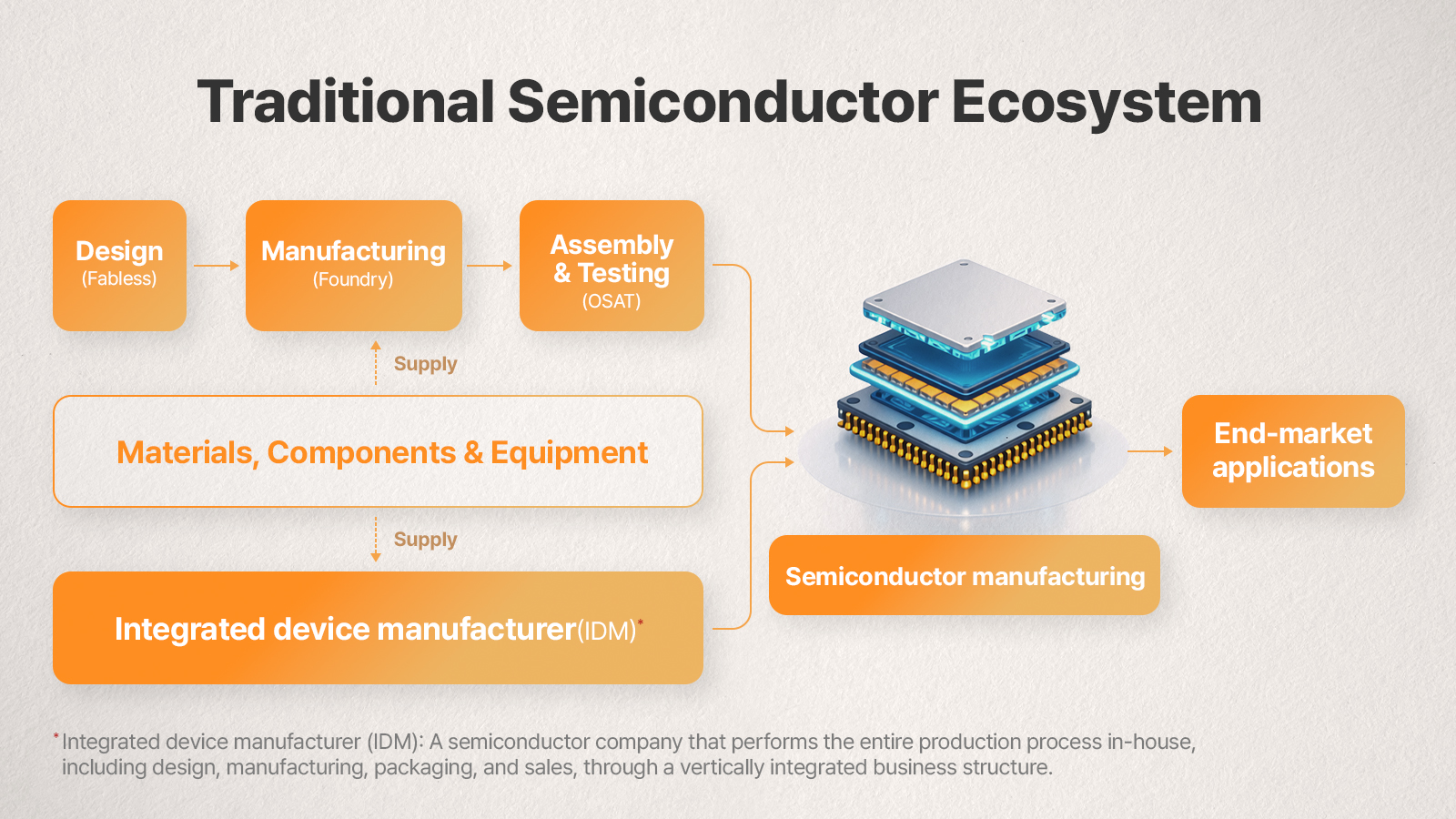
The semiconductor industry has long been built around a highly specialized ecosystem spanning design (fabless*), manufacturing (foundry*), assembly and testing (OSAT*), and end-market applications. Within this structure, each segment has focused on improving efficiency and expertise within its own part of the value chain.
* Outsourced Semiconductor Assembly and Test (OSAT) :A business model in which packaging, assembly, and testing are performed by specialized third-party providers after wafer fabrication is completed. Fabless and foundry companies typically rely on OSAT providers for package assembly and functional testing.
As AI services scale, the semiconductor ecosystem is entering a period of transition. The performance, latency, power efficiency, and operating costs of AI systems are no longer determined solely by algorithms or software optimization. They are also shaped by the underlying semiconductor architecture, memory systems, packaging technologies, network infrastructure, and data center environments that support them.
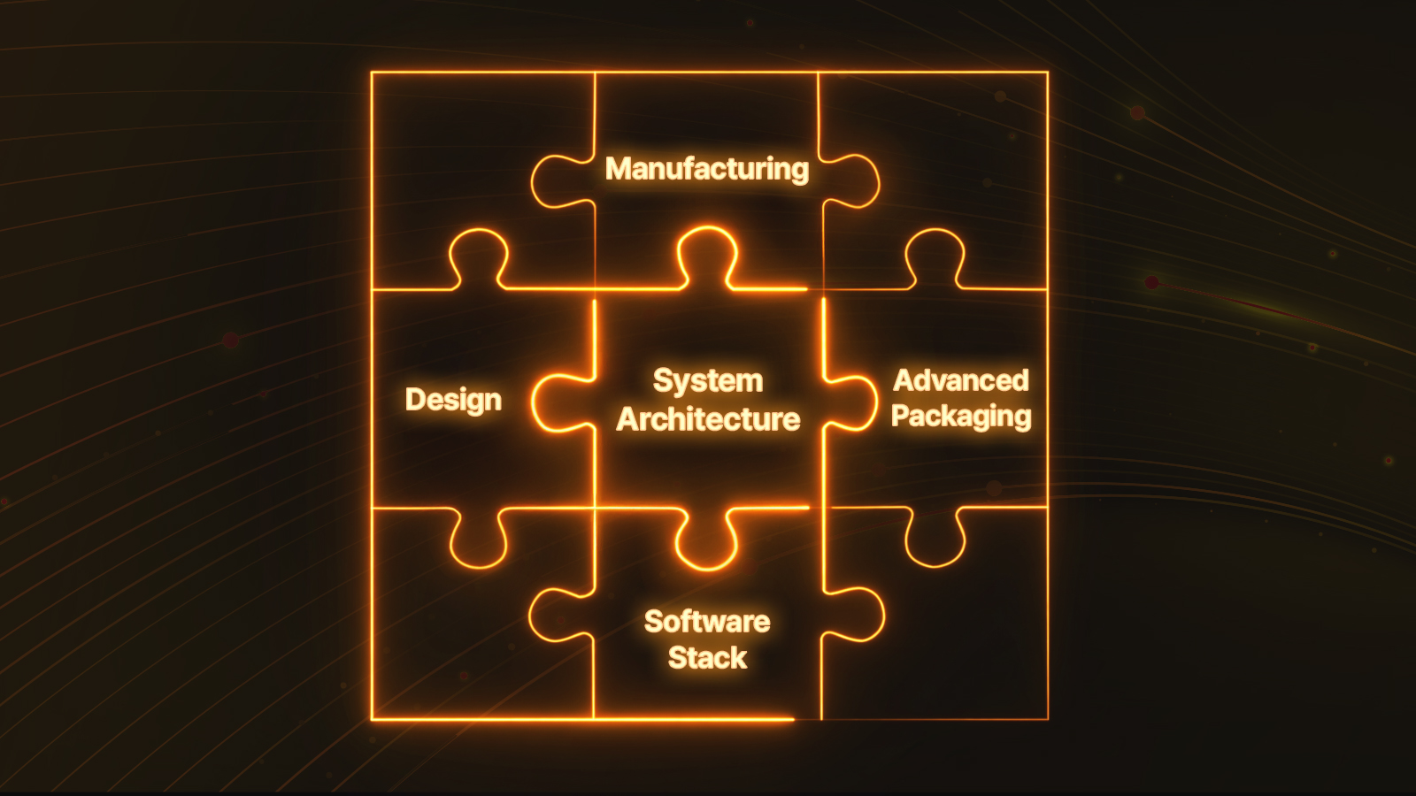
▲ AI semiconductors require a level of integration that extends across the entire technology stack — from design and manufacturing to advanced packaging, system architecture, and software stacks.
These requirements make AI semiconductors fundamentally different from conventional chips. From design and manufacturing to advanced packaging, system architecture, and software stacks, every layer of the technology stack must work together seamlessly. Only when that level of alignment* is achieved can performance and yield be improved consistently and reliably. This is also why partnerships between semiconductor companies and AI service providers are becoming more important.
As AI services continue to expand, performance and memory requirements are becoming increasingly diverse. Training, inference, generative AI, agentic AI, and on-device AI each place different demands on performance and memory. Some applications require extreme bandwidth, while others prioritize low latency and power efficiency. As a result, AI semiconductors and memory technologies are evolving toward greater optimization for specific workloads and system architectures.
This shift is also reshaping the role of memory companies. AI developers are no longer looking simply for faster memory. They increasingly require memory solutions optimized for specific AI workloads and system architectures. As a result, memory companies are expanding their role beyond product suppliers and becoming technology partners that work with clients from the earliest stages of system design — collaborating on performance, efficiency, power consumption, and packaging architectures.
From chips to platforms: The rise of integrated AI ecosystems
These changes are expanding competition in the semiconductor industry from a product-centric approach to a platform-centric one. In the past, semiconductor development typically began with the introduction of a new chip, followed by the expansion of applications built around it. Today, however, infrastructure strategies for AI services increasingly drive decisions about semiconductor specifications and investment timing from the very beginning, reversing the traditional development flow.

▲ NVIDIA is focusing not only on product development and manufacturing, but also on platform strategies that integrate the technologies required to deploy AI. (Source: NVIDIA)
This shift is already visible across the global market. NVIDIA is moving beyond its role as a GPU supplier with a full-stack strategy that integrates AI-accelerated computing, networking, and software. Its approach — spanning DGX systems* and cloud services — aims to bring semiconductors, systems, infrastructure, and services together within a unified architecture. In this model, NVIDIA is no longer simply selecting the highest-performance memory available. Instead, it begins with the AI platform it intends to build and then defines the memory requirements needed to support it. Semiconductors are no longer viewed as standalone products but are increasingly being designed as foundational elements of AI platforms.
The same trend can be seen elsewhere in the AI ecosystem. U.S.-based AI cloud company GMI Cloud is building an AI data center valued at approximately $500 million, a facility expected to deploy large numbers of GPUs and AI semiconductors. “To develop a regional ecosystem, you first need to build data centers and create AI clusters,” emphasized Alex Yeh, founder and CEO of GMI Cloud, underscoring how infrastructure assets such as data centers are becoming strategic assets in the AI era.
As competition in AI services intensifies, companies are focusing not only on developing algorithms but also on securing the large-scale computing infrastructure required to run them. Consequently, semiconductor demand in the AI era is no longer a matter of individual chips alone but an infrastructure challenge centered on large-scale computing clusters that combine tens of thousands of GPUs with vast amounts of memory. These developments underscore how semiconductors are evolving beyond intermediate industrial products to become essential building blocks that shape the performance of AI models and services.
Why memory optimization matters for AI services
For AI service providers, success depends not only on model performance but also on service costs, response times, power efficiency, and reliability. Delivering on these priorities requires more than powerful GPUs and AI accelerators. HBM, DRAM, advanced packaging, networking, and storage must all be optimized as part of an integrated system.
Within this architecture, HBM serves as the critical memory layer that delivers massive volumes of data to AI accelerators at high speed. As AI services become more sophisticated, companies must optimize custom HBM alongside memory-logic integration, advanced packaging, low-power DRAM, and high-capacity storage. Each plays a distinct role in addressing customer-specific challenges related to AI workloads, data movement, power efficiency, and system scalability.
AI memory competition is moving beyond generational improvements in speed, capacity, and cost efficiency. The priority now is optimizing workload-specific performance, power efficiency, and data movement across the system. Memory is becoming a more important part of AI infrastructure, supporting the real-world performance of AI services rather than competing solely on general-purpose specifications.
SK hynix: Evolving from supplier to technology partner
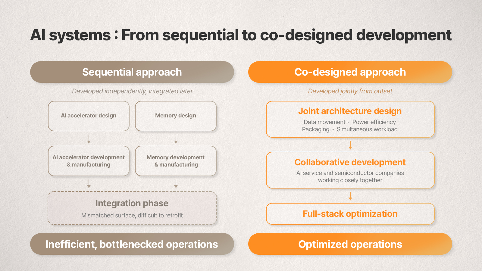
▲ Conventional development vs Co-designing from the outset
A key concept amid this transformation is co-design. Co-design brings AI accelerators and memory together from the earliest stages of architecture development, rather than treating them as separate components that are developed independently and integrated later. This approach considers data movement, power efficiency, packaging methods, and workload characteristics as part of the same design process from the outset. This is why collaboration between AI companies and semiconductor companies is becoming more important.
SK hynix’s focus on custom HBM, next-generation HBM, advanced packaging, and memory-logic integration is closely aligned with this shift. As AI infrastructure grows more complex, clients increasingly need memory partners capable of delivering performance and efficiency optimized for AI memory, system architectures, and service objectives.
In this environment, full-stack AI memory companies such as SK hynix are expanding their role beyond semiconductor suppliers to become key technology partners that co-design AI systems. Competitiveness in the AI era will no longer be defined by the performance of individual chips alone. It will increasingly depend on the ability to co-design and optimize entire systems and services. Ultimately, competition in the AI era is expanding beyond chips and toward ecosystems, with integrated platforms seamlessly connecting semiconductors and AI services at the core.
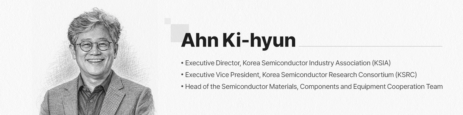
*This column was contributed by an external expert to provide insights into the AI semiconductor industry. The views expressed are those of the author and do not necessarily reflect the official position of SK hynix.