


SK hynix, which is leading the global memory market with its cutting edge semiconductor technologies, has been recognized by the Korean government for its contributions to the advancement of science and technology in the country.
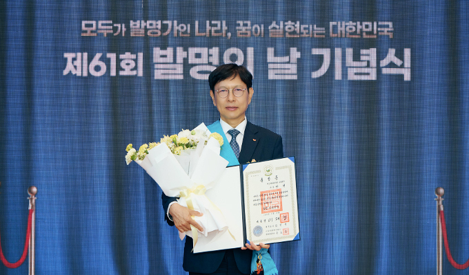
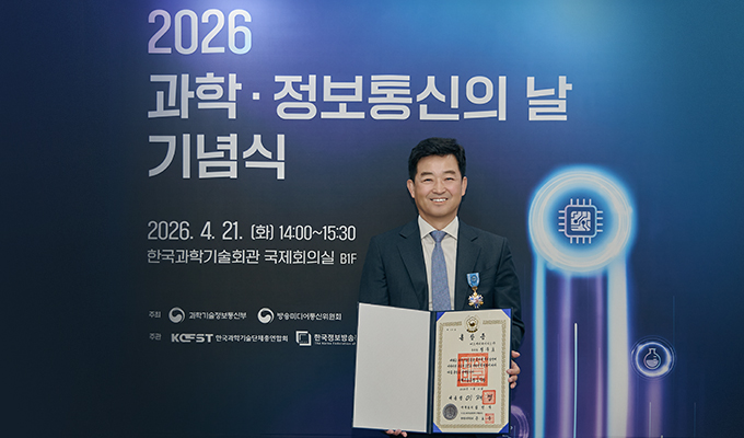
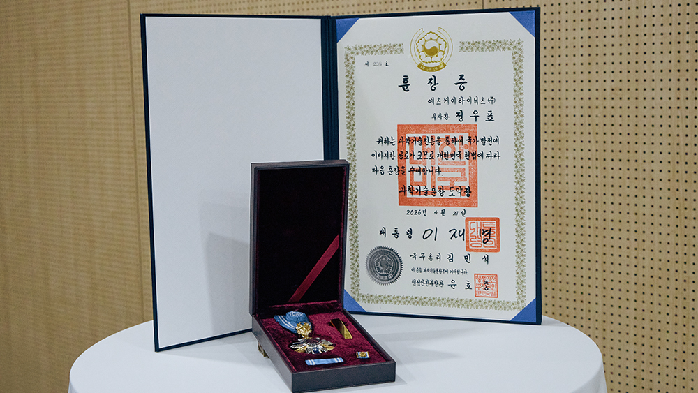
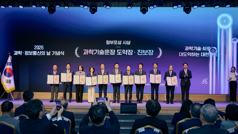
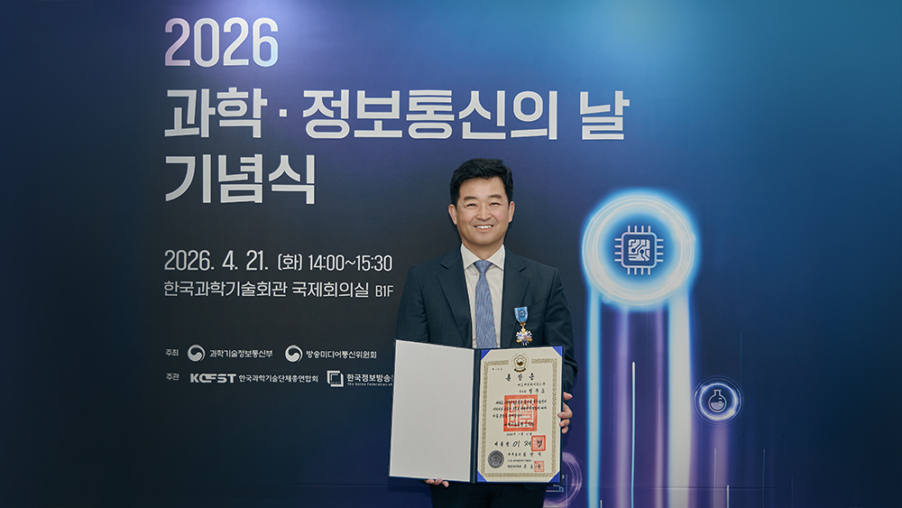
SK hynix announced that Vice President Woopyo Jeong, head of NAND Development, received the Order of Science and Technology Merit, Doyak Medal at the 2026 National Science and Information and Communications Day ceremony held on April 21 at the Korea Science and Technology Center in Yeoksam-dong, Seoul.
The ceremony was held to mark the 59th National Science Day (April 21) and the 71st Information and Communications Day (April 22), with the aim of instilling pride and a sense of honor among science and ICT professionals by presenting government awards to individuals who have contributed to the promotion of science, technology, and information and communications, as well as those recognized for their achievements in national R&D performance evaluations. Each year, the government holds a ceremony to honor individuals who have made outstanding contributions to the advancement of science and technology.
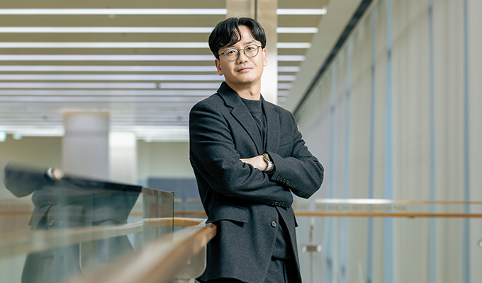
Vice President Jeong was recognized for enhancing Korea’s memory semiconductor competitiveness by achieving multiple world first developments over his 33-year career in DRAM and NAND development, contributing to the advancement of the nation’s industrial growth.
Strengthening National Semiconductor Competitiveness by Leading World-Class Memory Development Technologies
During the first 15 years of his career, Vice President Jeong participated in DRAM development, leading the world’s first development of 512Mb mobile DRAM and playing a pivotal role in establishing Korea as a dominant force in the global DRAM market. Over the following 18 years, he devoted himself to NAND development, leading the development process across eight consecutive generations—from the second generation (32-layer) 3D NAND to the ninth generation (321-layer) 4D NAND—elevating Korea’s memory semiconductor technology capabilities to world class levels.
In particular, Vice President Jeong has driven technological innovation by delivering outstanding results at critical inflection points in overcoming the limits of NAND stacking. In 2011, he drew industrywide attention by leading the world’s first development of 21-nanometer NAND with improved performance over the previous generation. He then went on to achieve world first developments of the second generation (32-layer), third generation (48-layer), and fourth generation (64-layer) NAND in succession starting from 2014, spearheading market trends during the transition from 2D to 3D NAND architecture. Notably, the 1Gbps ultra high speed operating circuit and low power circuit design technologies secured during this process served as a catalyst for expanding the applications of 3D NAND.
Furthermore, beginning with the world’s first development of the 128-layer sixth generation NAND in 2019, he achieved world leading read and quality performance with the 176-layer seventh generation NAND in 2021. In 2022, he successfully developed the 238-layer eighth generation NAND with the industry’s smallest chip size and was the first to commercialize the 512Gb capacity, demonstrating the company’s technological superiority. In 2024, he led the world’s first development of the 321-layer ninth generation 1Tb TLC1 NAND—currently the tallest in existence—once again pushing the boundaries of 4D NAND technology.
1A type of memory cell used in NAND flash. NAND flash is categorized as single-level cell (SLC, 1 bit), multi-level cell (MLC, 2 bits), triple-level cell (TLC, 3 bits), and quadruple-level cell (QLC, 4 bits) depending on how many data bits can be stored in one cell. As the amount of information storage increases, more data can be stored in the same volume.
In addition, Vice President Jeong overhauled the simulation methods used in design and independently developed an FPGA2-based verification tool to strengthen verification capabilities, advancing memory semiconductor design methodologies. These improvements in overall design efficiency and completeness significantly shortened the development timeline for next generation memory products, contributing to their timely introduction to the market.
2FPGA (Field Programmable Gate Array): A semiconductor that allows users to design and implement custom circuits. It is used to simulate various conditions during new product testing and solution verification processes.
Currently, Vice President Jeong is spearheading the effort to secure technological leadership and commercialize next generation NAND and its derivative products—the ‘AIN-P/B/D3’ family—in response to surging memory demand driven by the AI era. He is also strengthening national semiconductor competitiveness through industry academia partnerships with leading Korean universities, focusing on securing foundational semiconductor technologies and nurturing talented professionals.
3AIN-P/B/D: AIN is a portmanteau of AI and NAND, while P/B/D stands for Performance, Bandwidth, and Density, respectively. AIN-P refers to NAND for next-generation high-speed eSSDs; AIN-B refers to HBF (High Bandwidth Flash), which applies TSV technology used in HBM to NAND; and AIN-D refers to ultra-high-capacity NAND designed to replace HDDs in server applications.
“This Achievement Was Made Possible by Our Employees’ Dedication… We Will Respond with Memory Optimized for the AI Era”
Vice President Jeong remarked, “The driving force behind our ability to be the first to overcome technical barriers and deliver next generation products to market on time has always been the dedication and effort of my colleagues who showed unwavering commitment on the ground.” He added, “This order is not a personal honor but one I receive on behalf of all the employees who are writing the history of technological innovation at SK hynix.”
He cited ‘completeness’ and ‘execution’ as the values he considers most important in the development process. “The reason we worked so hard to advance our design methodologies and innovate our verification tools was to deliver products of the highest quality at the exact time our customers needed them,” he explained. “The secret to maintaining our leadership at every technological inflection point was the alignment of clear goal setting with the resolute execution of our employees.”
He continued, “In the coming AI era, memory semiconductors will go beyond simply storing data—the key will be how quickly and efficiently they can support AI models.” He added, “The AIN family we are currently preparing will be SK hynix’s answer to this market trend.”
Lastly, Vice President Jeong shared his aspirations: “As scaling limits approach and stacking technologies become more advanced, entirely new approaches beyond conventional methods will be needed.” He continued, “Together with our employees, I will continue to strengthen forward looking research and industry academia collaboration to ensure that Korea maintains its ‘technological supremacy’ in the global semiconductor market.”