At the TSMC Open Innovation Platform(OIP) Conference, held on the 23rd(local time) in Santa Clara, California, US, SK hynix shared its next-generation memory portfolio and development strategy, and reaffirmed its solid partnership with TSMC by receiving the Partner of the Year Award for the second consecutive year.
OIP is an open innovation platform operated by TSMC to develop technologies and collaborate with the companies that together make up the semiconductor ecosystem. Each year in the second half, TSMC invites OIP member companies and major customers to its ecosystem forums held around the world, fostering active technological exchange. SK hynix has taken part in the OIP Forums since 2024, introducing its evolving AI memory technology capabilities developed through its strategic partnership with TSMC.
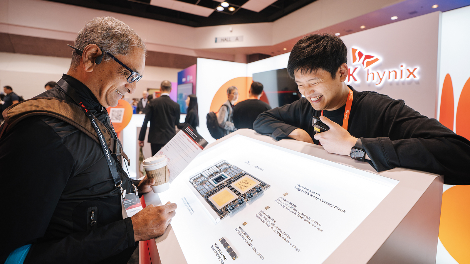
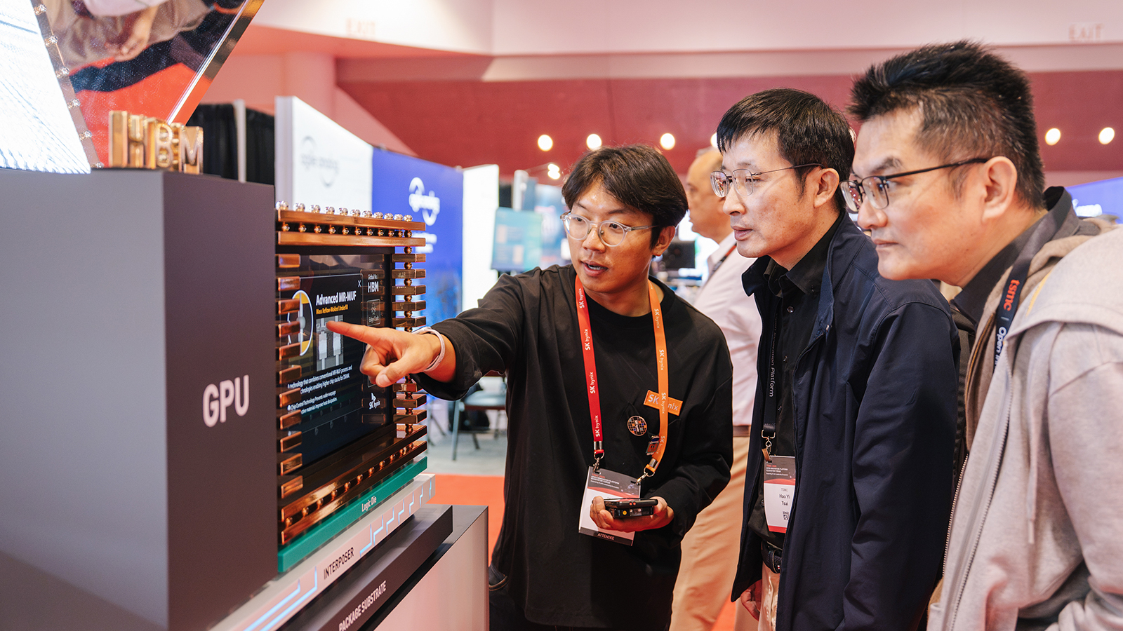
In today’s AI semiconductor ecosystem, collaboration between companies has grown closer than ever. The era in which design and manufacturing, memory and logic were each optimized within their own domains has given way to an approach in which companies design and validate together from the earliest stages. Held amid this shift, this year’s TSMC OIP Conference offered an opportunity to examine the latest technology development trends and explore new opportunities for collaboration. SK hynix, for its part, focused on showcasing its technological capabilities and product lineup while further defining and expanding its collaborative relationships with TSMC and other key partners.
Meeting SK hynix Inside the Superchip — Demonstrating HBM Capabilities That Have Advanced Alongside AI
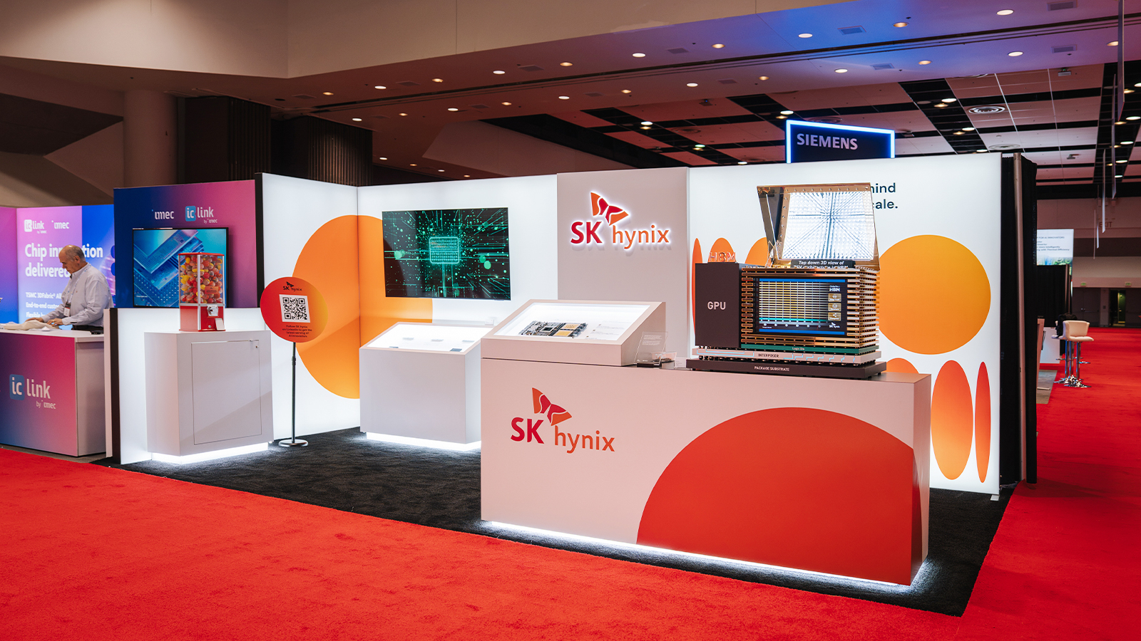
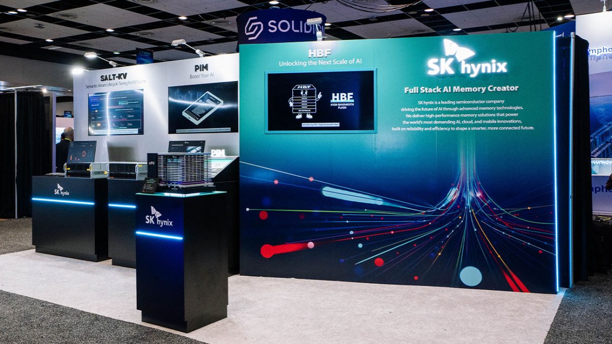
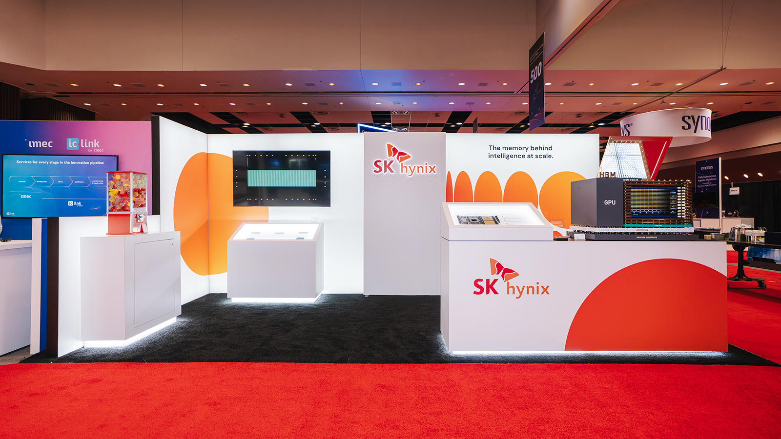
▲ The SK hynix booth design, carrying a message that emphasizes the importance of memory in the AI era
SK hynix presented “The Memory behind the Intelligence at Scale” as the slogan for this exhibition. The message captured the industrywide trend in which AI technology is advancing and its fields of application are rapidly expanding, while emphasizing that sustaining this growth depends on the support of memory technology. This message was reflected in the exhibition’s composition as well, which presented a range of memory solutions across different layers — from HBM* to server DRAM and eSSD — that support AI computation and data storage.
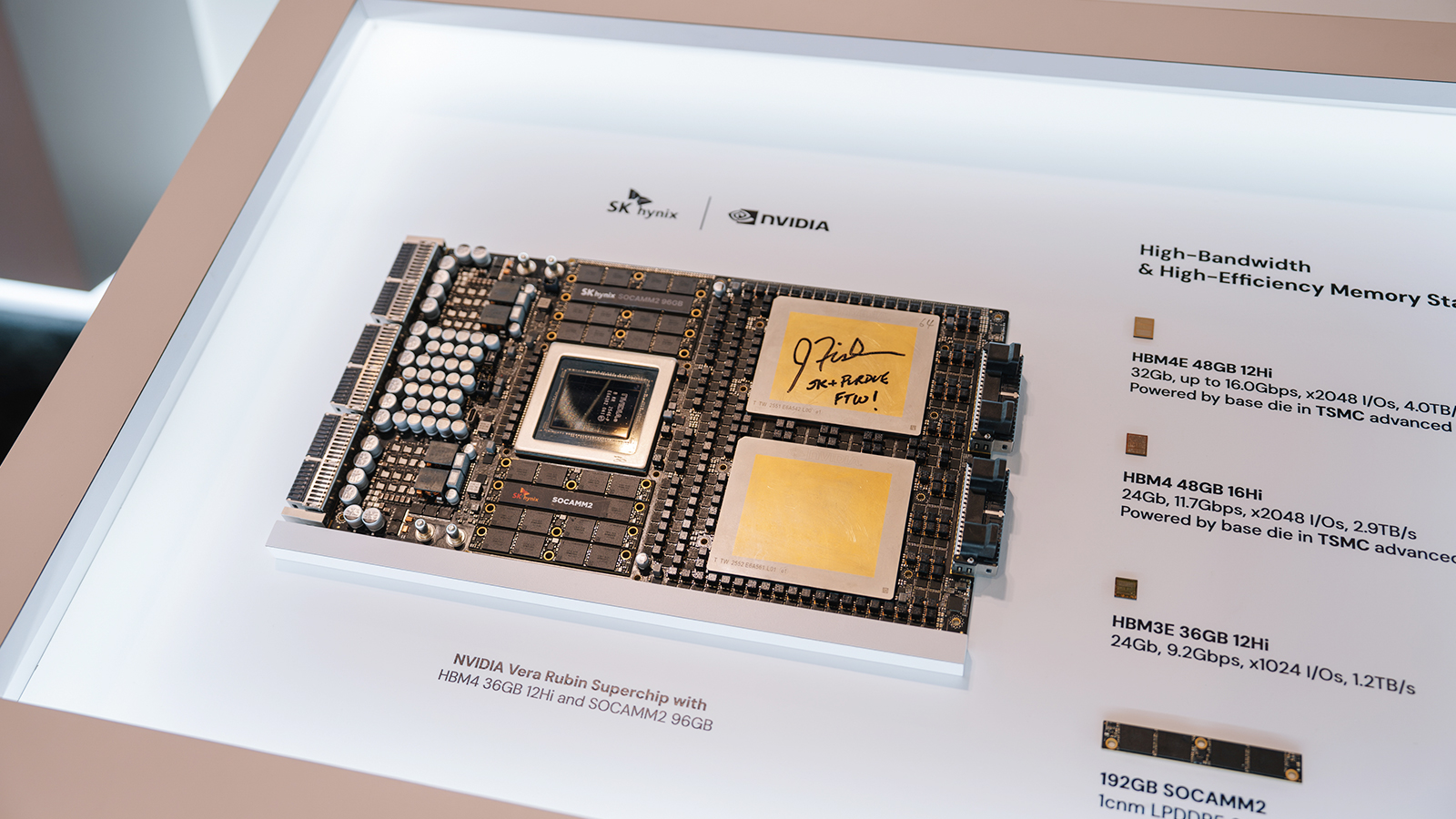
▲ NVIDIA’s superchip “Vera Rubin,” equipped with SK hynix’s 12-layer 36GB HBM4 and 96GB SOCAMM2
The product exhibition was organized into two main display stands: HBM and AI-optimized Memory and Storage. On the HBM stand, which visitors encountered immediately to their right upon entering the booth, NVIDIA’s superchip “Vera Rubin” was displayed together with SK hynix’s 12-layer 36GB HBM4 and 96GB SOCAMM2* mounted on it, so visitors could examine them closely. Alongside it, explanatory text detailing the role of the SK hynix products within Vera Rubin helped deepen visitors’ understanding.
In practice, the 12-layer 36GB HBM4 is integrated directly around the Rubin GPU core, serving as a high-bandwidth data pathway that resolves the data transfer latency arising in complex matrix operations. SOCAMM2, meanwhile, operates as the main system memory for the Vera CPU, supporting the complex computational processes and the resulting data movement so that AI agents can immediately reflect the context of long conversations in their responses.
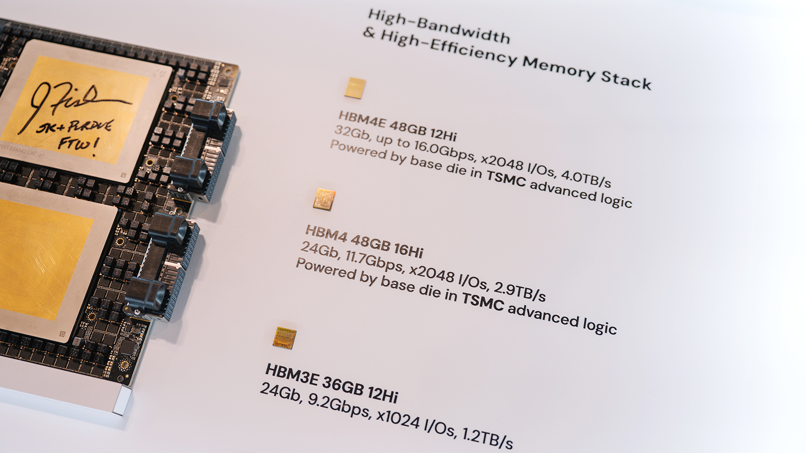
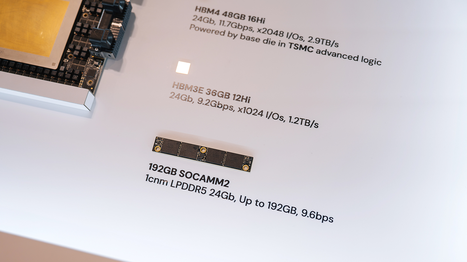
Around the superchip, key HBM products — the 12-layer 48GB HBM4E, the 16-layer 48GB HBM4, and the 12-layer 36GB HBM3E — were arranged side by side with an actual 192GB SOCAMM2 unit. By comparing the products already mounted in an AI accelerator with the next-generation lineup displayed beside them, visitors could see firsthand
SK hynix’s HBM capabilities, which have steadily evolved in step with the advancement of AI technology.
From Server DRAM to SSD — Unveiling a Next-Generation Product Lineup for the AI Infrastructure Market
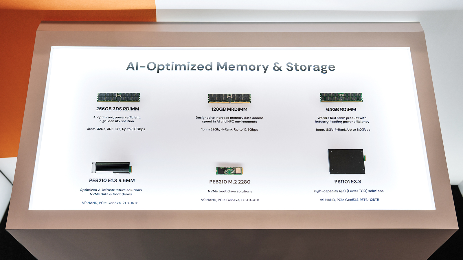
▲ SK hynix’s next-generation server DRAM lineup featured in this exhibition
On the left side of the booth, a display stand was arranged so visitors could view the next-generation server DRAM and SSD lineups in one place. The server DRAM lineup included the “256GB 3DS* RDIMM*,” which achieves the industry’s largest capacity tailored to AI workloads, along with the high-bandwidth “128GB MRDIMM*” and the “64GB RDIMM,” the world’s first to apply a 10-nanometer(nm) class sixth-generation(1c)* process.
* RDIMM(Registered Dual In-line Memory Module): A server memory module composed of multiple DRAM chips
* MRDIMM(Multiplexed Rank Dual In-line Memory Module): A product with significantly enhanced speed achieved by operating two ranks — the module’s basic operating units — simultaneously
* The 10-nanometer(nm) class process technology has progressed sequentially through generations 1x, 1y, 1z, 1a, 1b, and 1c(sixth generation)
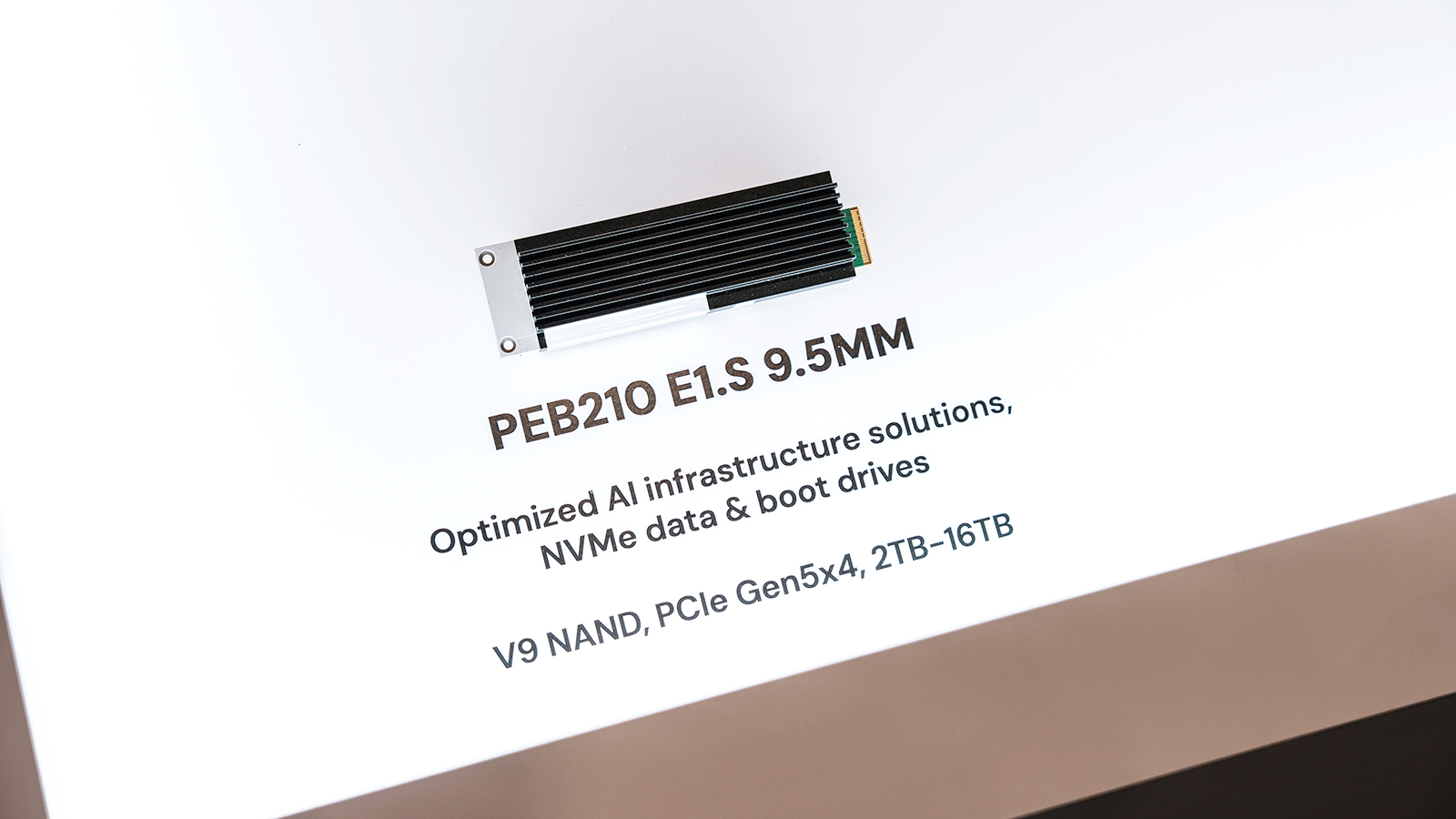
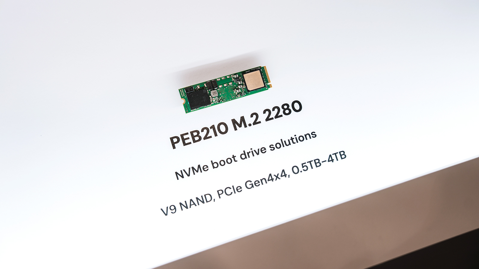
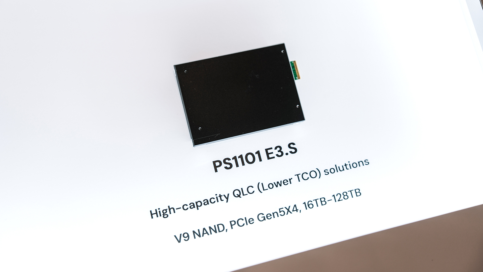
The SSD stand featured a lineup spanning different form factors and use environments — the PEB210 E1.S, the PS1101 E3.S, and the PEB210 M.2 — demonstrating SK hynix’s storage solution capabilities to meet a wide range of customer needs. The “PEB210 E1.S,” which supports Direct Liquid Cooling(DLC), drew strong interest from customers operating data centers, while the “PS1101 E3.S,” SK hynix’s first QLC*-based eSSD, prompted a steady stream of inquiries from enterprise customers.
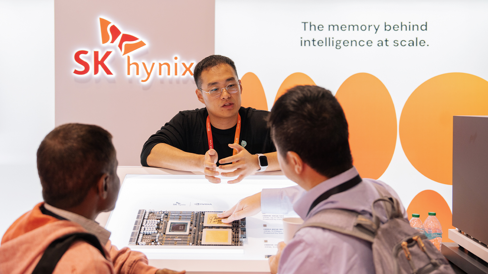
▲ A visitor at the SK hynix booth inquiring about detailed product information
Throughout the exhibition, SK hynix’s booth saw a constant flow of industry professionals eager to take a closer look at the AI memory solutions that form a core pillar of AI infrastructure. Company representatives also continued to visit to review SK hynix’s development plans and current technological capabilities, and to propose new collaborations on that basis.
Winning “Partner of the Year” for the Second Consecutive Year in Recognition of the HBM5 and CoWoS Collaboration
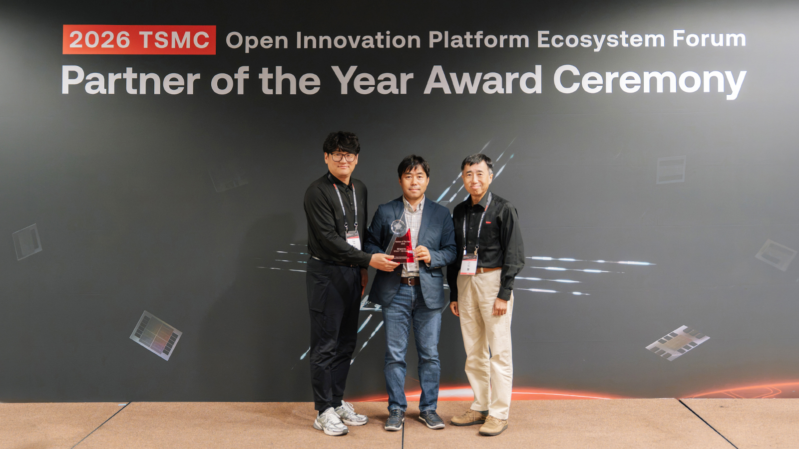
▲ (From left) Team Leader Jinwoo Park (PKG Product TE) and Vice President Jaesik Lee (Head of Advanced PKG Research), receiving the Partner of the Year Award on behalf of SK hynix at the TSMC OIP Conference
At this forum, SK hynix was named a Partner of the Year Award winner in the “3DFabric-HBM Integration” category. This marked the company’s second consecutive win following last year, this time in recognition of a collaboration that validated HBM5 on the basis of TSMC’s CoWoS* to advance next-generation AI systems.
As HBM advances through successive generations, raising its stack count and bandwidth, fully realizing these gains in performance requires close coordination with the advanced packaging technology that integrates it into an actual AI accelerator. It was here that
SK hynix’s Package Development organization and TSMC carried out validation together from the earliest stages, laying the foundation for next-generation AI systems — a collaborative relationship that led to this award.
From the Role of PCIe in the AI Era to the Next-Generation SSD Roadmap — Sharing a Vision for Technology Development in the Presentation Session
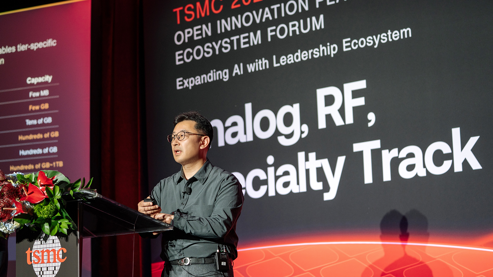
▲ Daesik Park, a distinguished engineer in PCIe Design, delivers a presentation
In the presentation session, Daesik Park, a distinguished engineer in PCIe Design took the stage as the second speaker in a joint presentation with Cadence, sharing changing market trends and SK hynix’s response under the theme “PCI Express Solutions for HPC/AI Storage,” and introducing the AI memory technologies being developed to address them.
Park first outlined the technological shifts underway in the PCIe* field. “Since the fourth generation, a new generation has arrived every two to three years, doubling bandwidth each time, and from the sixth generation in particular, power optimization and collaboration between design and process have become even more important,” he explained. “As new memory layers — including HBM and HBF* — take shape to improve AI and GPU performance, PCIe has emerged as the key interface connecting these layers to GPUs, CPUs, and networks.”
* HBF(High Bandwidth Flash): A next-generation NAND-based memory technology being discussed as a new memory layer between HBM and SSD. Like HBM, it applies a logic process to the base die, providing far greater capacity than HBM while securing comparable bandwidth and cost efficiency
He also shared market projections and SK hynix’s response. “As AI infrastructure expands, the PCIe-based eSSD market is expected to grow roughly 3.8 times, from 509EB* in 2026 to 1,933EB in 2030,” Park said. “As demand grows for high capacity, high density, and cooling efficiency, demand for the E1.S and E3 form factors will also rise rapidly.” He continued: “SK hynix has developed a wide range of SSD controllers using TSMC processes since third-generation PCIe, and for the sixth and seventh generations we are preparing next-generation SSD solutions based on chiplets*. The design separates the conventional single-chip controller into chiplet* units connected via UCIe*, which is expected to enable shorter development times, independent generation transitions for each function, capacity expansion, and power optimization.”
* Chiplet: A technology that divides one large chip by function into several smaller chips, then connects them within a single package. Because each function can be developed and combined independently, it shortens development time and enhances design flexibility
* UCIe(Universal Chiplet Interconnect Express): An open standard interface for connecting different chiplets within a single package
SK hynix stated, “By winning the Partner of the Year Award for the second consecutive year at this OIP Conference, we once again confirmed the results of the collaboration we have built with TSMC.” The company added, “We will continue to work closely with a range of partners to create the memory solutions the AI era demands.”