As AI workloads evolve toward inference and agentic AI, the criteria for system performance are also changing. Computing power alone is no longer enough. Where data is stored, how quickly it moves, and how efficiently it is processed now have a direct impact on the performance and efficiency of AI systems.
This article series explores the transformation of the AI ecosystem, where software, data center infrastructure, semiconductors, and memory technologies work together. It also examines why memory semiconductors have become a foundational technology for the AI era and outlines SK hynix’s vision for building the next-generation AI memory ecosystem.
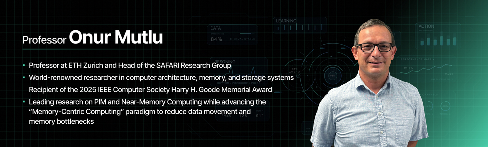
Part 3 draws on the perspective of Onur Mutlu, a globally renowned expert in computer architecture and professor at ETH Zurich, who has long studied DRAM performance and reliability as well as memory-centric computing. It explores why AI infrastructure is increasingly prioritizing architectures that minimize data movement over faster individual components.
① The paradigm shift in AI computing
② The real bottleneck: Data, not compute
③ Redesigning infrastructure: Why architecture determines performance
– Professor Onur Mutlu, ETH Zurich
④ The semiconductor paradigm shifts toward memory
⑤ Completing AI: Physical intelligence and the role of memory
From faster components to systems that move less data
For a large language model(LLM) service such as ChatGPT, Gemini, or Claude to answer a single question, the model must repeatedly access vast amounts of model weights, previous context, and intermediate results. As responses become longer and involve more reasoning steps, the amount of data that must be read also increases. Therefore, one of the key challenges for AI systems has been how quickly and reliably they can supply massive volumes of data to compute devices.
This challenge has become increasingly important as the center of gravity in AI shifts from model development to large-scale service operations. Pre-training requires a massive upfront investment, while inference occurs repeatedly every time a user submits a query. As generative AI services, enterprise copilots, and agentic AI proliferate, the number of requests grows, and the context that each request must maintain becomes longer. As a result, AI infrastructure competition is moving beyond simply deploying faster GPUs/NPUs/TPUs and larger clusters. The focus is increasingly on how efficiently GPUs/NPUs/TPUs, memory, storage, and networks can be co-designed and connected as an integrated system and how efficiently data can flow through that system. Or more appropriately, how minimally the system moves data across components.
The cost of data movement in processor-centric architectures
Today’s computing systems provide a very powerful infrastructure that has enabled increasingly important workloads such as AI and machine learning, genomic analysis, and large-scale data analytics. Yet their fundamental architecture remains processor-centric. Data must continuously move across the memory hierarchy — from sensors, storage, memory, and caches all the way to the compute device(s) and back again — before and after being processed.
This architecture has long been effective at improving the performance of general-purpose computations. As AI workloads have grown dramatically in both data volume and access frequency, however, data access and data movement have become major bottlenecks in system efficiency. Models continuously access vast amounts of weights and intermediate results, while inference repeatedly reads previous context and newly generated tokens. The farther and more data must travel, the greater the latency, power consumption, and hardware cost.
To mitigate these data access and data movement bottlenecks, system designers have complicated the design of computers greatly. Modern computing systems employ many complex and expensive mechanisms, such as cache hierarchies*, prefetching data before it is needed, multithreading to execute multiple tasks in parallel, and out-of-order execution*. These technologies have had limited effectiveness at reducing the latency of compute devices, but they have come at significant complexity, energy inefficiency, and hardware cost in the system.
* Out-of-order execution: A technique that reduces compute device idle time by executing instructions that are ready to execute ahead of others, even when this differs from the order specified in the program
In today’s computing systems, computation is relatively cheap, yet memory access and data movement are expensive — in both performance and energy. The energy required to retrieve data from DRAM once can be 150 to 2,000 times greater than that required for a simple arithmetic operation. Research involving neural network models running on Tensor Processing Unit(TPU) systems has demonstrated the huge energy and performance impact of this disparity*. For large machine learning models, more than 90% of system energy can be consumed by memory access and data movement rather than computation*.
* Onur Mutlu et al., “A Modern Primer on Processing in Memory,” in Emerging Computing: From Devices to Systems – Looking Beyond Moore and Von Neumann, Springer, 2022; updated 2025
The compute-memory disparity becomes even more pronounced with large language models(LLMs). Each time an LLM generates a token, it refers to the previous context and handles vast amounts of intermediate data through the KV cache* and attention operations. As models reason for longer periods and maintain longer contexts, their requirements for memory capacity and bandwidth* drastically increase. The memory bottleneck becomes larger and larger as these memory demands increase. No matter how fast the compute device becomes, system efficiency declines because the system spends most of its time waiting for data to arrive at the compute units.
As AI workloads scale, High Bandwidth Memory becomes increasingly important for supplying GPUs with larger volumes of data at higher speeds. Positioned next to the GPU/NPU/TPU, HBM delivers large amounts of data at ultra-high speeds, helping reduce compute device latency. To fully utilize HBM performance, however, the entire data path must be designed as an integrated system — not only the GPU/NPU/TPU and HBM, but also storage, networks, and interconnects*.
* Memory Bandwidth: The amount of data that can be transferred from memory within a given period of time. Higher memory bandwidth allows compute devices to receive and process more data at once
* Interconnect: A communication pathway connecting system components such as processors, memory, accelerators, and storage. In AI infrastructure, interconnects are a key factor in determining the speed and efficiency of data movement
Why system architecture matters more than component speed
The fundamental assumptions behind system design also need to change. Processor-centric architectures largely operate by moving data to compute devices for processing. As data volumes grow and access frequency increases, architectures that send all data to a central compute device quickly reach their limits. Now, the system must instead be redesigned around where data resides and the path it takes to be processed.
One concept developed to address this challenge is memory-centric computing*. Solving the memory bottleneck in a fundamentally better way requires reducing data movement and enabling computation closer to memory. This is the basic idea behind memory-centric computing. Memory-centric computing takes data location and movement costs as key considerations in system design, optimizing memory placement and compute architecture together*. Some data may reside in HBM next to the GPU/NPU/TPU, while other data is managed in a shared memory pool*, with certain computations performed closer to memory. The best approach depends on factors such as model architecture, context length, the number of user requests, and network configuration.
The good news is that such memory-centric systems are already being designed and evaluated not only in academia but also in the industry. There is an increasing push toward eliminating data movement bottlenecks, and this is best done by not moving data as much as possible.
* Onur Mutlu, et al., “Memory-Centric Computing: Solving Computing’s Memory Problem,” 17th IEEE International Memory Workshop(IMW) (2025)
* Memory pool: A shared memory resource that can be accessed by multiple devices. By allowing each device to use memory capacity as needed, memory pooling can improve overall system resource utilization
High-speed interconnects: The two pillars of memory expansion and GPU connectivity
Processors, memory, and accelerators have long been connected through a variety of interfaces. As the volume of data processed by AI workloads grows rapidly, however, conventional connectivity architectures are struggling to provide the required communication bandwidth and memory access efficiency. Consequently, the importance of high-speed interconnects that enable faster and more flexible data paths between devices is increasing. Today, CXL* and NVLink/NVSwitch* are two representative technologies driving this shift in different areas and various academic works to tightly integrate components exist.
* NVLink and NVSwitch: High-speed interconnect technologies developed by NVIDIA. NVLink provides high-bandwidth connections between GPUs or between GPUs and other devices, while NVSwitch extends this connectivity to enable high-speed communication among larger numbers of GPUs. These technologies are used to reduce GPU-to-GPU data bottlenecks in large-scale AI clusters
CXL is a key interconnect technology that enables memory expansion and sharing. In traditional server architectures, memory has largely functioned as a dedicated resource attached to a specific CPU or GPU/NPU/TPU. Even when one device had spare memory capacity while another faced a shortage, it was difficult to share that capacity flexibly. CXL expands connectivity among processors, accelerators, and memory devices, providing a foundation for flexible memory expansion, sharing, and pooling. With CXL, computation can also be offloaded to devices or controllers that perform processing near memory, while CXL devices can communicate with one another through the flexible interface.
NVLink and NVSwitch provide high-bandwidth connectivity within GPU clusters. When large-scale AI models run across multiple GPUs and nodes, intermediate data such as model parameters, activations, and the KV cache must move between GPUs. If GPU-to-GPU connectivity is slow or inflexible, overall processing performance can suffer regardless of how fast each individual GPU is.
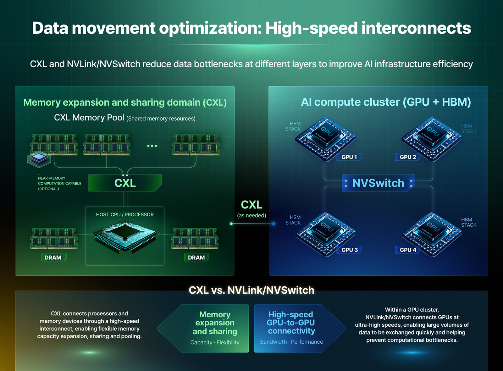
CXL and NVLink/NVSwitch serve different roles: CXL focuses on memory expansion and sharing, while NVLink/NVSwitch provide high-bandwidth GPU connectivity. Both, however, support the same broader goal of reducing data bottlenecks in AI infrastructure by enabling the delivery of the required data quickly to where it is needed. When such a connection architecture is established, memory and accelerators cease to become fixed components and become system resources that can be configured around workload requirements.
The flexible connectivity enabled by high-speed interconnects is also changing how compute devices and memory are arranged. As more data paths become available between devices, compute and memory resources can be positioned according to workload requirements. This shift points toward an architecture that does not simply move more data over longer distances but instead performs the required processing closer to where the data resides.
Tightly connected near-memory accelerators: Processing data closer to memory through cooperative computing
Reducing data movement bottlenecks can go a step beyond simply increasing connection speeds. While CXL and NVLink/NVSwitch improve data paths between memory and GPUs/NPUs/TPUs in different ways, near-memory acceleration reduces the amount of data that must be moved by placing computation itself closer to the data.
Instead of having a central GPU/NPU/TPU retrieve and process all data, accelerators located in or near memory devices divide the workload among themselves. These accelerators are tightly coupled through high-speed interconnects, allowing data to be processed close to memory first, with only the necessary results exchanged with other devices, rather than sending the entire dataset to a central GPU/NPU/TPU. When computation takes place near 3D-stacked high-bandwidth memory* such as HBM or other high-capacity memory, much less data needs to travel back and forth. This can reduce latency and power consumption while making it easier to scale across multiple nodes. This architecture is known as a distributed system of tightly connected near-memory accelerators*.
The potential of this approach can be seen in Tesseract*. Tesseract is a research architecture(published at the 42nd ACM/IEEE International Symposium on Computer Architecture in 2015) that applies distributed near-memory acceleration to parallel graph processing. Multiple accelerators located close to memory process their assigned data independently and communicate with one another only when necessary. For various parallel graph-processing workloads, the research demonstrated an order-of-magnitude performance improvement along with a similar energy reduction compared with conventional processor-centric designs.
The significance of these results extends beyond the numbers themselves. By processing each node’s assigned data locally and reducing communication volume, the architecture can achieve greater scalability and energy efficiency than conventional designs. As more and diverse accelerators are added, memory capacity, memory bandwidth*, and computation capability all scale proportionally. In other words, the key is not simply distributed processing, but an architecture in which multiple near-memory accelerators are tightly connected and perform computation cooperatively with minimal data movement.
* Distributed system of tightly connected near-memory accelerators: An architecture that connects multiple accelerators located close to memory via high-speed interconnects, enabling each accelerator to process its assigned data and exchange only the necessary results
* Tesseract: A research architecture for near-memory acceleration in which multiple accelerators located close to memory are tightly connected through high-speed interconnects. Each accelerator processes its assigned data locally and communicates with others only when necessary
* The original architecture is published at the 42nd ACM/IEEE International Symposium on Computer Architecture in 2015, with a paper entitled “A Scalable Processing-in-Memory Accelerator for Parallel Graph Processing”.
More recently, research has also targeted LLM inference. For example, a CXL-based LLM inference study presented at ASPLOS* 2025 demonstrated how memory expansion architectures and processing units located close to memory can help to greatly alleviate capacity and bandwidth constraints in large-scale inference infrastructure(called the CENT design)*. As memory capacity and bandwidth requirements increase, architectures that concentrate all computations on a central GPU/NPU/TPU alone face growing challenges in improving efficiency. Such distributed near-memory architectures like the CENT design that minimize data movement using near-memory processing and efficient & scalable interconnects in intelligent and novel ways can improve all metrics(performance, energy, cost, hardware area) at the same time.
* Yufeng Gu, Alireza Khadem, Sumanth Umesh, Ning Liang, Xavier Servot, Onur Mutlu, Ravi Iyer, and Reetuparna Das, “PIM Is All You Need: A CXL-Enabled GPU-Free System for Large Language Model Inference,” ASPLOS 2025
Disaggregated architecture: Resource pooling and workload-optimized allocation
Disaggregated architecture* starts from the same fundamental challenge but takes a somewhat different approach. Unlike near-memory accelerator architectures, which move computation closer to data, disaggregated architectures organize CPU, GPU/NPU/TPU, memory, storage, and network resources into a system-wide shared pool. In this structure, the necessary resources can then be flexibly combined according to workload requirements. Workloads that require large memory capacity can use an expanded memory pool, while workloads whose performance depends on bandwidth can be handled by near-memory accelerators. In essence, resources are deployed according to the workload’s requirements rather than being fitted into a fixed server configuration. This is very much in-line with the “Asymmetry Everywhere” vision outlined in 2010 to enable customized, flexible, and reconfigurable processing to maximize energy efficiency and performance*.
* Onur Mutlu, “Asymmetry Everywhere(with Automatic Resource Management),” CRA Workshop on Advancing Computer Architecture Research, 2010
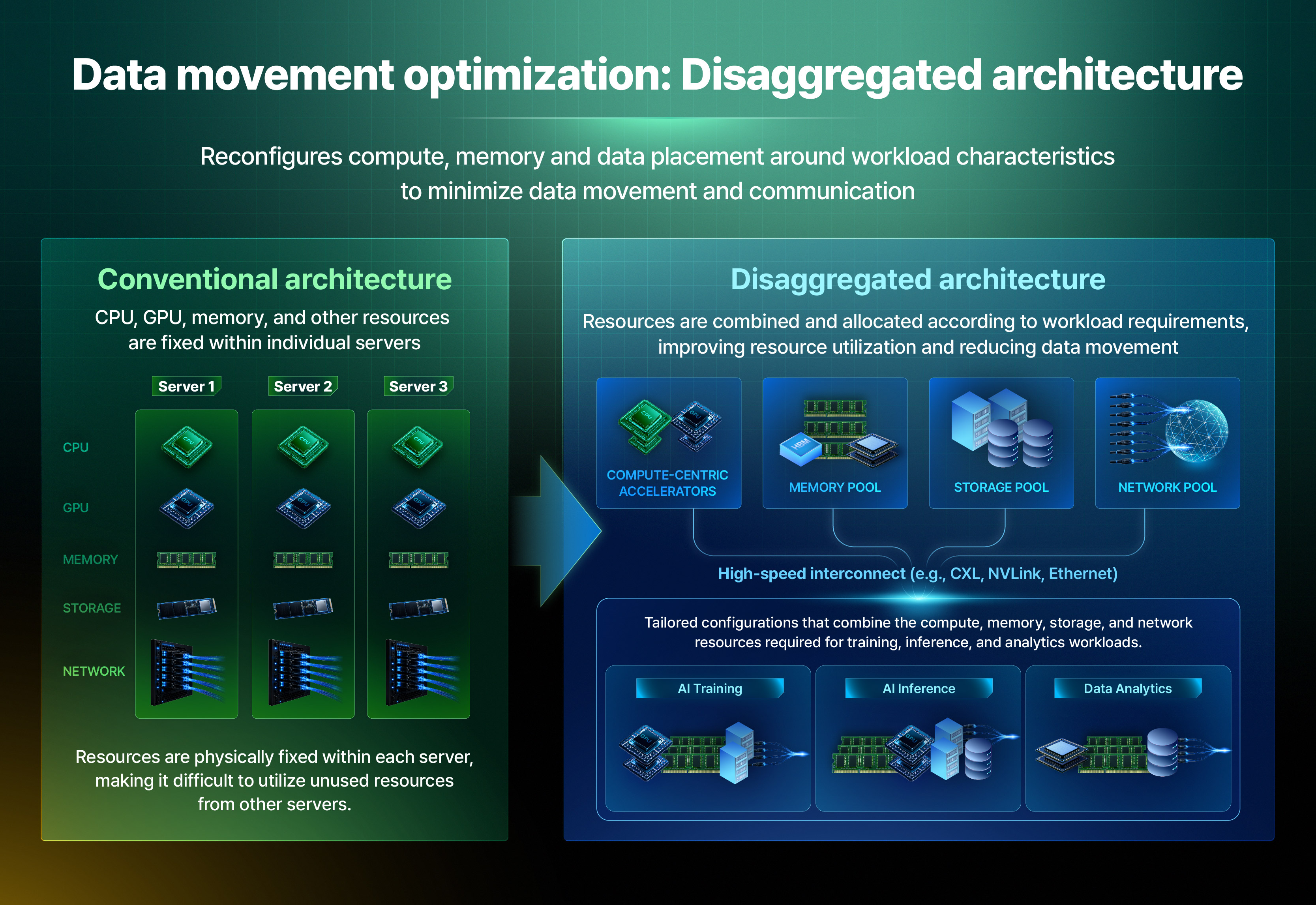
Data that requires substantial memory capacity, such as the KV cache, and memory-intensive operations, such as the attention layer*, are representative use cases for this type of architecture. With high-speed, flexible interconnects and flexible, compute-capable memory configurations, these workloads can be assigned to separate memory resources or near-memory acceleration domains. This reduces the burden on GPUs/NPUs/TPUs to retrieve and process all data directly, while allowing devices to locally and efficiently perform computations and to exchange results more efficiently.
The effectiveness of a disaggregated architecture depends on balancing resource allocation with communication costs. How to minimize communication and how to perform efficient data flow within and across accelerators continue to be important questions because excessive communication can actually increase latency and energy consumption. It is therefore critical to determine which resources and workloads should be disaggregated, which should remain close to memory, and where exactly what computation should be performed.
Reconfigurable AI infrastructure
The competitiveness of AI infrastructure depends on how fast and efficient a path it can provide to the data required for computation. High-speed interconnects such as CXL and NVLink, near-memory accelerator architectures such as Tesseract, and disaggregated architectures that flexibly and efficiently combine computation and memory resources according to workload requirements, including CXL-based memory pooling and customized near-memory processing, are all moving in this direction. This is also why major Big Tech and cloud companies continue to invest heavily in AI infrastructure architecture. The economics of AI competition now extend beyond acquiring more compute devices to how efficiently one can design AI systems across the stack with memory as a first-class citizen: enabling efficient use of memory, power, networks, silicon, and minimizing data movement to greatly improve inference performance and efficiency.
This shift is transforming AI infrastructure from static infrastructure into a dynamic system. As models grow and evolve, contexts lengthen, and inference calls increase, infrastructure must become more flexible and efficient. It must be able to select the appropriate processing path for each workload and model.
As system architectures rapidly evolve, so does the role of memory. Traditionally, memory has primarily been treated as a device for storing and supplying data. With AI workloads, however, the distance between where data resides and where computation takes place directly affects performance and power efficiency. Accordingly, memory is quickly evolving to become an active first-class citizen to perform computation and improve overall system efficiency.
Recent research results are particularly fascinating, showing that some computation is already possible within existing DRAM chips themselves*. By changing how the memory controller* accesses DRAM and activating multiple rows simultaneously, systems can perform large-scale(TeraOps per second* level) bit-level operations or data copying & initialization purely inside modern DRAM chips. These capabilities arise from the fundamental operational principles of DRAM circuitry itself. We call this approach processing using DRAM, since one “uses” (existing) DRAM chips to perform computation. This recent discovery on the extensive computational capabilities of real DRAM chips offers only a glimpse, yet an important one, of how memory could take on a more active role in future computing architectures and provides a foundation for building new processing-in-DRAM mechanisms into future DRAM chips and standards.
AI performance cannot be fully explained simply by adding up the specifications of individual components. Future competitiveness will increasingly depend on how precisely systems are designed and how computation is performed around where data resides, which devices perform computation, and which paths are used to exchange results.
* Memory controller: A device that controls data read and write commands and timing between the processor and memory
* Tera Operations Per Second(TOPS): A throughput metric that measures the number of operations performed per second in trillions. One TOPS represents one trillion operations per second; here, it refers to the scale of bit-level operations performed within DRAM
Next: Why is the semiconductor paradigm shifting toward memory?
Bottlenecks in AI infrastructure arise not only from individual components such as GPUs or memory, but especially from how computation is distributed and communication is performed, i.e., from how GPUs/NPUs/TPUs, HBM, storage, networks, and interconnects exchange data. The major bottleneck we face today is the huge amounts of data movement caused by the processor-centric paradigm. High-speed interconnects, near-memory accelerator architectures, and disaggregated architectures explored above are all system-level approaches to reducing the large burden of data movement.
Now, the question turns to the architecture of semiconductors and memory themselves. Beyond simply placing data closer to compute devices, how much more data movement could be reduced if some computations were performed within or around memory itself?
The next article will explore why the center of gravity in AI semiconductors is shifting toward memory, with a focus on HBM, advanced packaging, and processing-in-memory(PIM).
Disclaimer: The opinions expressed in this article are solely those of the author and do not necessarily reflect the official position of SK hynix.