SK hynix offers a full-stack portfolio of AI memory solutions optimized for AI systems across all major memory categories, including High Bandwidth Memory(HBM), DRAM, and NAND flash.
To highlight the research that underpins these solutions as well as the company’s broader technology roadmap, the SK hynix Newsroom is launching an article series titled [Inside the Research].
Part 2 explores an approach that co-optimizes cell, non-cell, and page schemes to improve the efficiency of 3D FeNAND-based analog compute-in-memory(A-CiM).
[Read the paper]
· Title: “Co-Optimizing Cell, Non-Cell, and Page Schemes for Energy Efficient Analog Computing in 3D FeNAND”
· Published in: 2025 IEEE International Electron Devices Meeting(IEDM)
· Authors: Won-Tae Koo & Jihun Kim, Technical Leader, Global RTC, SK hynix
(Summary) | (Full Text)
Research background: The need for a new type of NAND for AI computing
As large-scale AI models continue to grow, the power consumption and latency associated with data movement are emerging as major bottlenecks in AI infrastructure. To address these challenges, SK hynix’s research team focused on analog compute-in-memory*, an architecture that combines data storage and computation, and proposed an approach based on 3D FeNAND* that co-optimizes cell, non-cell, and page schemes.
AI computing performance can no longer be explained by the speed of compute devices alone. Where data is stored, where computation takes place, and how much data movement can be reduced all have a direct impact on overall system efficiency. Against this backdrop, compute-in-memory is gaining attention. CiM reduces the burden of data movement by processing data within or close to memory rather than continuously transferring it to compute devices.
* 3D FeNAND: A 3D NAND architecture that incorporates ferroelectric properties. It uses the polarization state of ferroelectric materials to store data and control current states
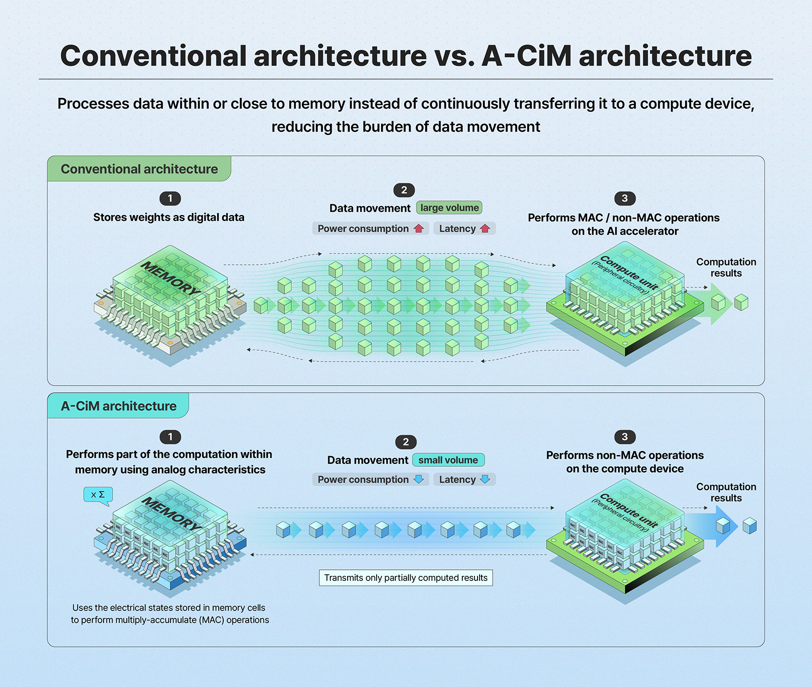
Among these approaches, A-CiM uses the electrical states stored in memory cells to perform multiply-and-accumulate* operations, a fundamental building block of AI computation. As AI models grow, so does the volume of weight data that must be stored and repeatedly accessed. As a result, architectures capable of storing large amounts of data at a high density are becoming an essential requirement for implementing A-CiM.
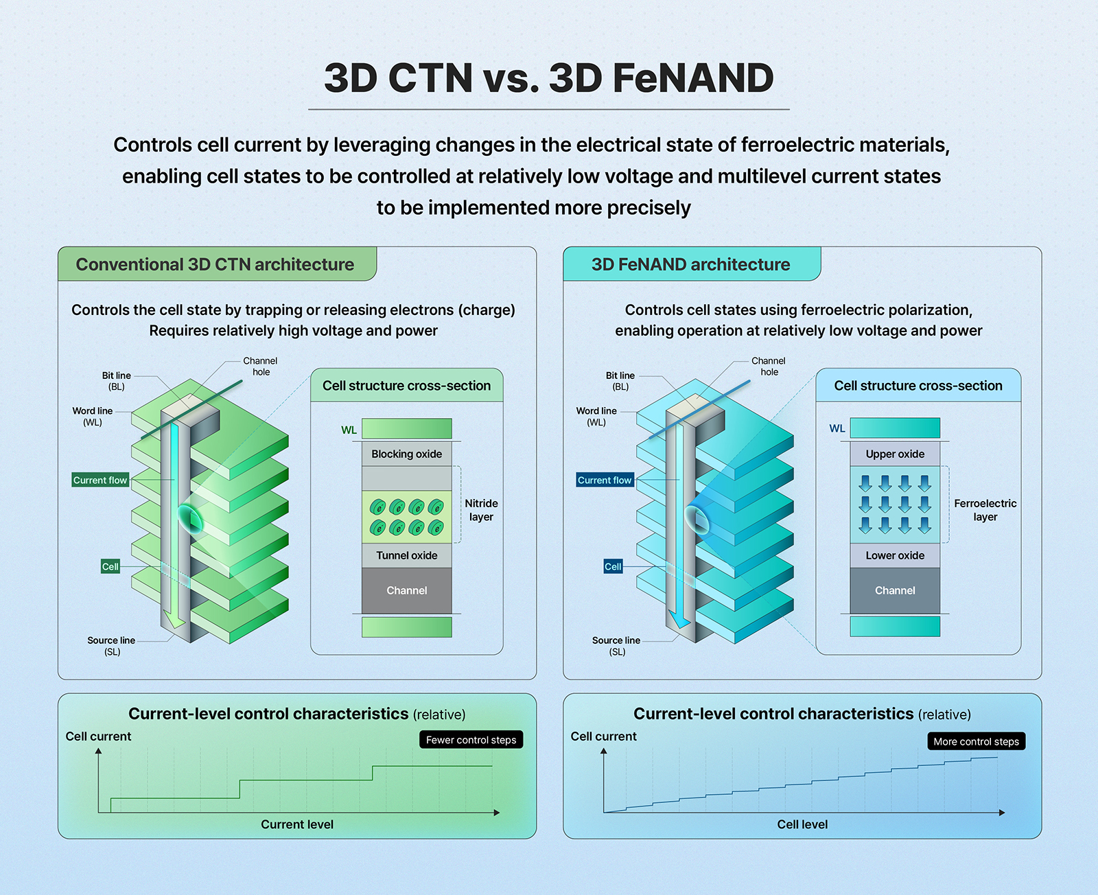
The research team identified 3D FeNAND as a memory architecture well suited for A-CiM. Commercial 3D NAND primarily uses a charge trap nitride(CTN) structure, which controls cell states by trapping or releasing electrons within a nitride layer. While this structure offers advantages in terms of density, it has limitations when it comes to precisely distinguishing the multiple current levels required for analog computing.
FeNAND, by contrast, controls cell current by leveraging changes in the electrical state of a ferroelectric* material. Ferroelectric materials retain their internal polarization state even after an external electric field is removed. By changing this polarization state, data can be stored and the state of a memory cell can be controlled. These properties give FeNAND an advantage over conventional 3D CTN NAND in precisely controlling multiple current levels at a lower power.
However, applying 3D FeNAND to A-CiM requires more than simply changing the cell structure alone. Even if cells can reliably distinguish between different current levels, overall performance remains limited if significant power is lost in the interconnects used to select and control them. Likewise, even if the interconnect burden is reduced, failing to utilize pages in alignment with the AI model’s data size and computation sequence can introduce unnecessary switching and latency.
This is why the cell, non-cell, and page schemes need to be co-optimized. To translate the potential of 3D FeNAND into practical A-CiM efficiency, current-level control at the cell level, word line* switching overhead, and page utilization must be improved together within a single integrated architecture.
Research results: Co-optimizing cell, non-cell, and page schemes
What distinguishes this research is its holistic approach to optimizing the cell, non-cell, and page schemes together rather than improving each separately. In A-CiM, cells must precisely represent multiple current levels, while non-cell components must minimize power loss when selecting and controlling those states. The page scheme organizes the data used for computation into appropriate sequences and units to reduce unnecessary switching operations.
If a bottleneck remains in any one of these three areas, overall performance is constrained. Even if cells can precisely represent values, high word line switching overhead reduces power efficiency. Likewise, even if interconnect overhead is reduced, inefficient data organization within a page can increase latency. Applying a holistic co-optimization* approach across all three areas improved the computational throughput and energy efficiency of 3D FeNAND-based A-CiM.
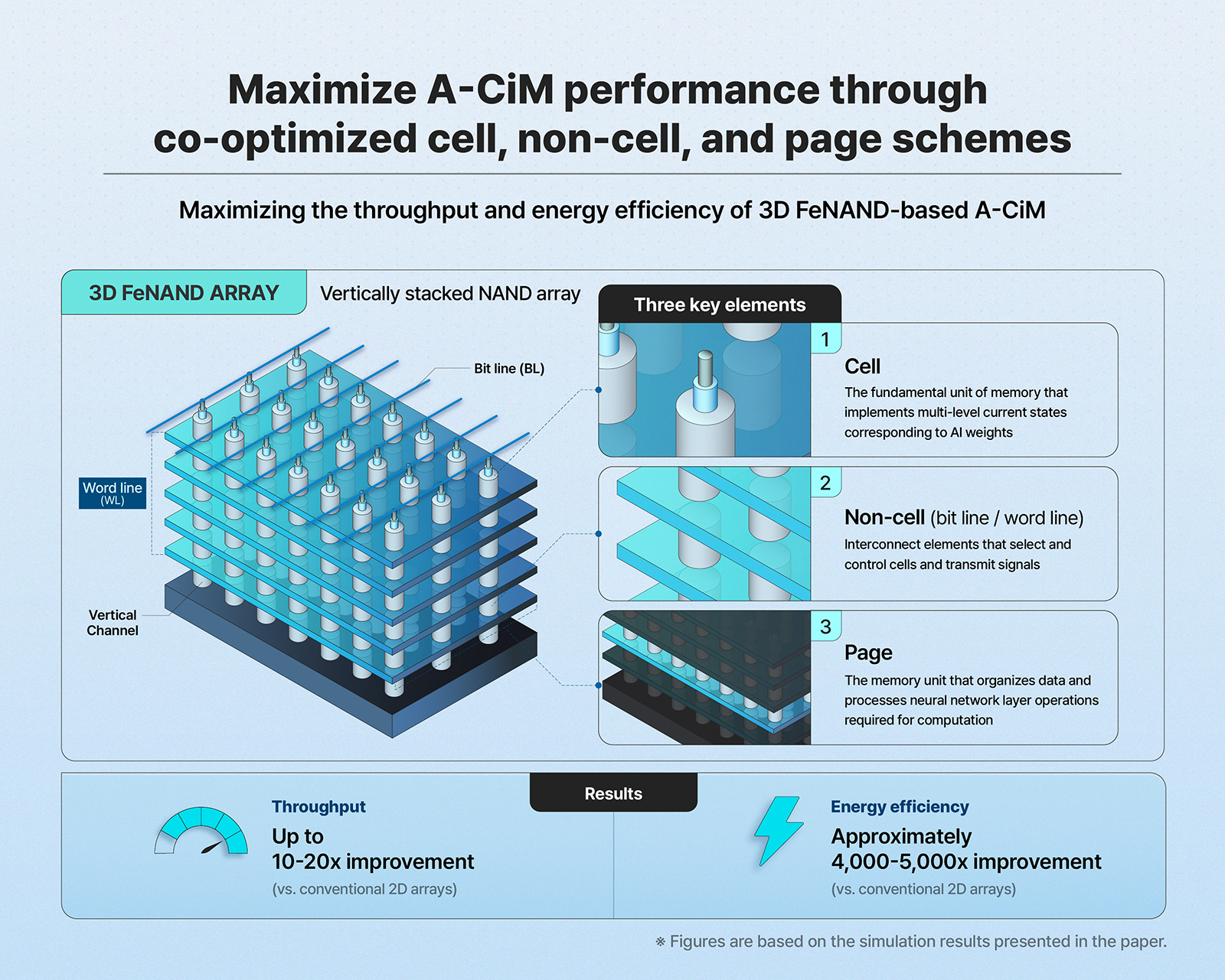
The benefits of co-optimization have been demonstrated quantitatively. The optimized 3D FeNAND architecture significantly improved throughput and energy efficiency compared with conventional 3D NAND-based architectures. Under the same chip-area constraints, it also delivered approximately 10 to 20 times higher throughput and around 4,000 to 5,000 times greater energy efficiency than conventional 3D arrays. These gains reflect the high integration density of 3D FeNAND and the reduction in data movement achieved through co-optimization of the cell, non-cell, and page schemes.
The results suggest that performance improvements beyond what can be achieved through higher memory density alone can come from system-level optimization. AI computing efficiency is not determined solely by how much data can be stored. Overall performance also depends on how stored data is represented through different current states, how those states are controlled through interconnects, and in what sequence and units the data is used for computation.
The research is also significant in that it expands the potential role of NAND in AI systems. In the AI era, NAND is no longer limited to storing large volumes of data. It is evolving toward supporting high-density storage weights for large-scale AI models, reducing the energy burden associated with data movement and rewriting, and improving computational efficiency.
With its high integration density, low power consumption, and multi-level control capabilities, 3D FeNAND-based A-CiM demonstrates the potential for NAND to expand beyond a storage medium into a computing medium. In particular, the co-optimization of cell, non-cell, and page schemes demonstrates the potential to optimize NAND architectures at the system level to meet the requirements of AI workloads.
Research focus: Optimization strategies for cell, non-cell, and page schemes
The bottlenecks in 3D FeNAND-based A-CiM can be categorized into three areas — cell, non-cell, and page — each requiring a different optimization approach. The cell scheme determines how data is represented through different current states. The non-cell scheme covers the interconnects and peripheral structures used to select and control the cells. The page scheme concerns how data used in actual AI computation is organized into different units and sequences. Although these three areas may appear separate, they are closely interdependent during actual A-CiM operations.
☑︎ Optimization point 1: Cell – Precise control of multi-level current states
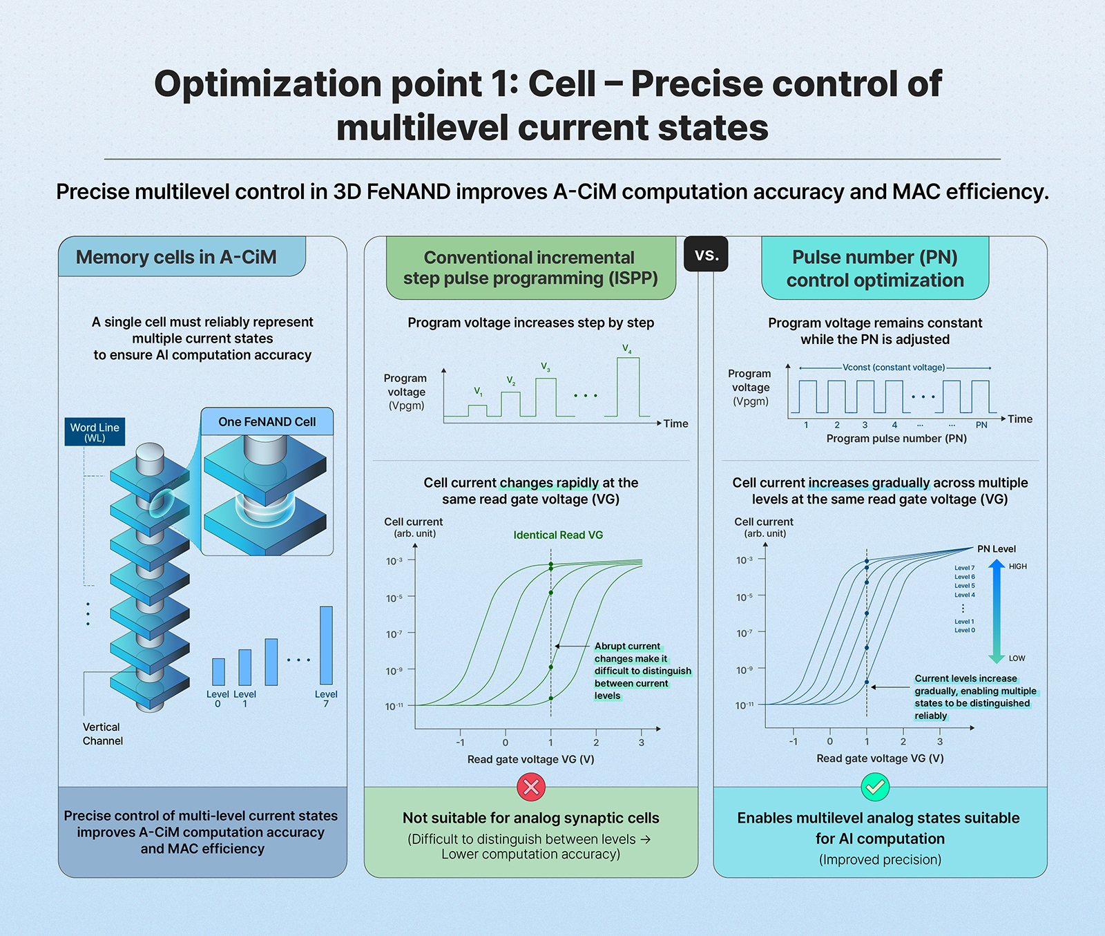
In A-CiM, memory cells do more than simply store 0s and 1s. To precisely store and compute AI model weights, each cell must reliably represent multiple current states. Without sufficient multi-level* capability, the precision of analog computation decreases, ultimately reducing the efficiency of MAC operations.
Conventional NAND primarily employs incremental step pulse programming* to precisely control threshold voltage*. ISPP controls the threshold voltage of a memory cell by incrementally increasing the programming voltage. However, this approach can cause abrupt changes in cell current at the same read gate voltage*. This characteristic is not well suited to analog synaptic cells, which require multiple current levels to be distinguished gradually and precisely.
For 3D FeNAND, the research team adopted an approach that increases the pulse number* at the same voltage while minimizing subsequent incremental increases in voltage. As the number of pulses increased, the threshold voltage gradually approached saturation, while the cell current measured at the same read gate voltage increased in distinct steps. This gradual response enables multiple analog states for AI computation.
* Incremental step pulse programming(ISPP): A method that adjusts the threshold voltage of a memory cell by progressively increasing the programming voltage
* Threshold voltage(Vth): The voltage at which current begins to flow through a memory cell. It varies depending on the stored charge or cell state and is used to read data
* Read gate voltage(VG): The voltage applied to the gate to read the state of a memory cell. Measuring how cell current varies at the same read gate voltage indicates how reliably the cell can distinguish between different analog states
* Pulse number(PN): The number of programming pulses applied to change the state of a memory cell. In this research, PN was adjusted to distinguish multiple cell current states
The advantages of FeNAND are also evident in how it controls current. Conventional CTN NAND changes the cell state by adjusting the amount of electrons stored in the nitride layer. FeNAND, by contrast, uses domain switching* in HZO*-based ferroelectric materials. This characteristic enables precise multi-level operation in the low-current region. Four-level-per-cell operation in the low-current region, along with stable data retention, was also demonstrated at the 300mm wafer scale.
* Hafnium zirconium oxide(HZO): A hafnium- and zirconium-oxide-based ferroelectric material used to control cell states in FeNAND
☑︎ Optimization point 2: Non-cell – Reducing word line switching overhead
The second challenge exists outside the cell itself. In NAND architectures, word lines are interconnects used to select and control memory cells. During MAC operations in A-CiM, selected and unselected word lines repeatedly switch states. This switching increases both power consumption and latency.
Word line resistance and capacitance were identified as key non-cell factors in 3D FeNAND arrays. Higher word line resistance and capacitance slow signal transmission and increase the energy required to switch between selected and unselected states. An important goal of non-cell optimization, therefore, is to reduce both factors and lower switching overhead.
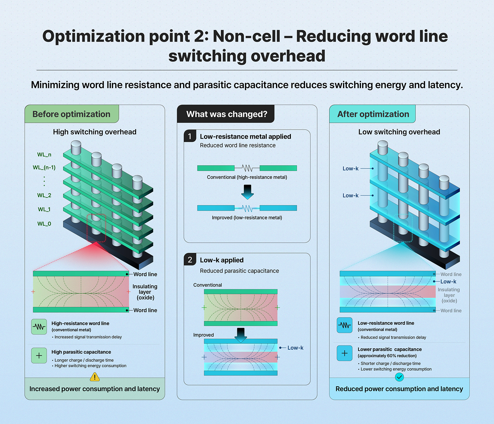
The analysis first examined how different word line metals affect performance. Compared with the baseline structure, using a low-resistance metal improved throughput by up to 16% and energy efficiency by up to 3%. The improvement in energy efficiency was relatively limited because overall power consumption is affected more by word line capacitance than by word line resistance.
The analysis then considered introducing air gaps* into the oxide between word lines to reduce parasitic capacitance*. Applying air gaps reduced parasitic capacitance between word lines by approximately 60%, improving throughput by 1.2 times and energy efficiency by two times. When word line resistance and capacitance were jointly optimized, throughput improved by up to 1.4 times and energy efficiency by up to 2.2 times.
Non-cell optimization improves the pathway that translates the analog states implemented in the cells into actual computation. Even with precise cell operations, the advantages of A-CiM diminish if switching word lines consumes excessive power and time. Reducing interconnect overhead alone, however, is not sufficient. Latency and the number of switching operations also vary depending on how the data used for computation is arranged within a page.
* Parasitic capacitance: Unintended electrical capacitance that occurs between closely spaced interconnects such as word lines. When voltage is applied to one interconnect, it can affect adjacent interconnects, increasing signal delay and power consumption
☑︎ Optimization point 3: Page – Optimizing computation sequence and data placement
The third challenge involves computation at the page level. A-CiM throughput depends heavily on how many inputs can be processed in parallel within a page or array. The number of page switches also affects throughput* and energy efficiency(TOPS/W)*. Even when large amounts of data can be stored, inefficient organization of the values used for computation can result in unnecessary switching and increased MAC latency.
The first page-level technique is in-page pipelining*. IPP efficiently organizes neural network* layers within a single page and, when appropriate, replicates layers to increase computational parallelism. IPP is also designed to reduce both the number of MAC operations and word line switching events.
Simulation results showed that IPP doubled energy efficiency and improved throughput by nine times compared with the baseline architecture. This demonstrates that how data is organized and processed within a page — both in sequence and units — has a direct impact on A-CiM performance.
The second page-level technique is page splitting*. Dividing a conventional 16KB page into four 4KB subpages enables data to be organized more flexibly according to the input and output sizes of neural network layers. Rather than using a single large page as one unit, dividing it into smaller units allows unused subpages to accommodate replicated layers or other neural network layers. As a result, fewer pages need to be assigned to a workload, thereby reducing switching energy, latency, and MAC latency.
* Tera operations per second per watt(TOPS/W): An energy efficiency metric representing the number of operations that can be performed per watt, measured in trillions
* In-page pipelining(IPP): A method that optimizes neural network layer placement and computation sequences within a single page to reduce the number of operations and word line switching events
* Neural network(NN) layer: A computational stage within an artificial neural network. Each layer receives inputs, performs computations using weights, and passes the results to the next layer
* Page splitting: A method that divides a large page into multiple smaller subpages so they can be used according to the input and output sizes of neural network layers
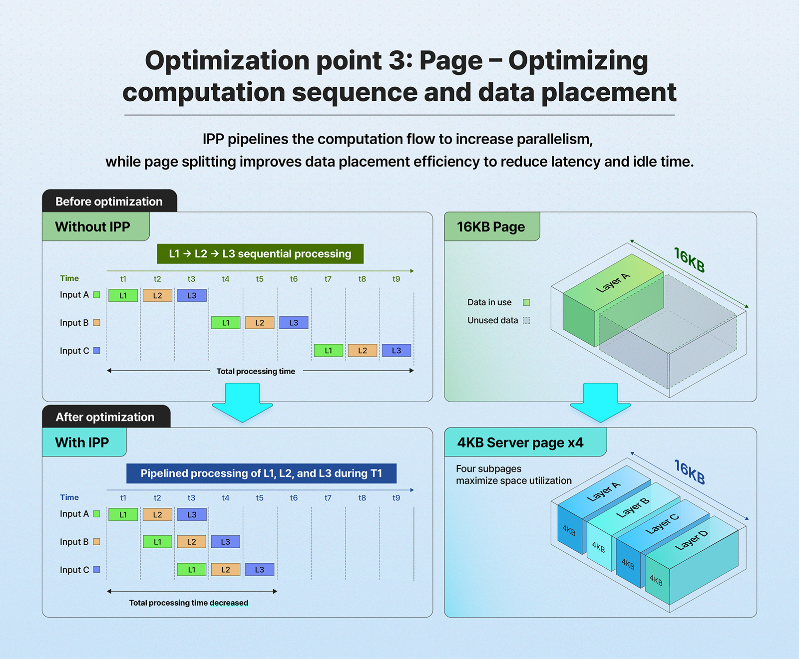
Applying page splitting improved energy efficiency by 1.2 times and throughput by 1.7 times. However, smaller page sizes do not always produce better results. The optimal page size varied across neural network models. If pages become too small, neural network layers may be divided into too many segments, which could instead increase MAC latency.
These results indicate that page optimization is not simply a matter of memory configuration, but of aligning AI model architecture with memory operation. The cell scheme precisely represents values, the non-cell scheme efficiently selects and controls those values, and the page scheme coordinates the delivery of data for computation in an efficient sequence. A-CiM performance ultimately depends on how effectively these three elements work together.
Easy to understand: A-CiM optimization through the analogy of an international airport
At its core, A-CiM aims to reduce the time and power consumed by repeatedly moving data. Using international airport operations as an analogy, 3D FeNAND is like a large hub airport capable of handling large numbers of passengers and flight schedules. A larger airport can accommodate more passengers, just as higher-density memory can store more data — but a larger facility does not automatically result in faster operations.
First, passengers must be accurately identified and assigned to the appropriate gates for their destinations. This is similar to cell optimization, in which a single cell must reliably distinguish between multiple current states to precisely represent the values used in AI computation. The more accurately this step is handled, the more smoothly the subsequent processes can proceed.
Next, transportation routes such as runways, taxiways, and boarding bridges must be designed for efficient movement. Complex routes or bottlenecks can delay overall airport operations. This corresponds to non-cell optimization, which reduces the overhead associated with the word lines and peripheral structures used to select and control cells. Making the paths through which current flows more efficient helps reduce power consumption and latency.
Finally, takeoff and landing schedules must also be coordinated. Even within the same airport infrastructure, poorly organized flight sequences and time allocation can increase waiting times. Similarly, A-CiM performance depends on the sequence and units in which data is arranged for computation. Ultimately, 3D FeNAND-based A-CiM can reduce the burden of data movement and improve AI computing efficiency when cell, non-cell, and page schemes are optimized to work together.
Interview: Researchers discuss the potential of 3D FeNAND-based A-CiM
Q1. How should we interpret the approximately 10-20x improvement in throughput and 4,000-5,000x improvement in energy efficiency reported in the paper?
These figures reflect the high-density advantage of 3D FeNAND compared with conventional 2D nonvolatile memory arrays, which have been widely studied as candidates for A-CiM. Under limited chip-area constraints, conventional 2D arrays have limited storage capacity and therefore require weights to be repeatedly reloaded, resulting in significant energy consumption from data movement and rewriting.
By contrast, 3D FeNAND can store more weights at once and use them directly for computation, reducing the need for reloading. This increases throughput while lowering energy consumption. The ability to perform more computation with less power within the same area is a key factor behind the performance improvements demonstrated in this research.
Q2. What was the most challenging technical issue you encountered during the research?
The most difficult aspect was that the issues we needed to address were not confined to a single area. Improving the performance of 3D FeNAND-based A-CiM required us to consider cell, non-cell, and page schemes simultaneously. Because this required a combined understanding of ferroelectric devices, NAND architecture, and AI workloads, it was a structural challenge that could not be addressed through expertise in any single field alone.
Overcoming this challenge required collaboration among researchers with diverse areas of expertise. Researchers in each area shared their optimization results and incorporated insights from other areas back into their own work. This ultimately enabled us to achieve co-optimization across cell, non-cell, and page schemes as a single integrated system.
Q3. What does this research suggest about the future direction of NAND technology?
This study suggests that NAND could evolve beyond a storage medium into a computing platform. In particular, FeNAND based on ferroelectric materials demonstrated higher energy efficiency than conventional 2D nonvolatile memory arrays and 3D CTN NAND, supporting its potential as a low-power, high-efficiency A-CiM platform.
This approach could extend beyond AI computation to other data-centric computing applications, including in-memory search. From the perspective of developing an ultra-high-density, low-power in-memory computing platform for large-scale AI models, this research presents a new direction for the evolution of NAND technology.