SK hynix showcased its advanced AI memory and data center products at the TSMC Open Innovation Platform (OIP) Ecosystem Forum 2024 held on September 25 in San Jose, California. The annual event brings together TSMC OIP1 members and the semiconductor design community to foster industry collaboration and drive innovation. At this year’s event, SK hynix strengthened its strategic partnership with the host TSMC based on HBM2 development and presented key products, including its HBM3E and the world’s first 1cnm DDR5 product.
1Open Innovation Platform (OIP): A comprehensive design technology infrastructure encompassing all areas of integrated circuit implementation which aims to promote innovation. Members include a variety of semiconductor design and manufacturing companies.
2High Bandwidth Memory (HBM): A high-value, high-performance product that revolutionizes data processing speeds by connecting multiple DRAM chips with through-silicon via (TSV).

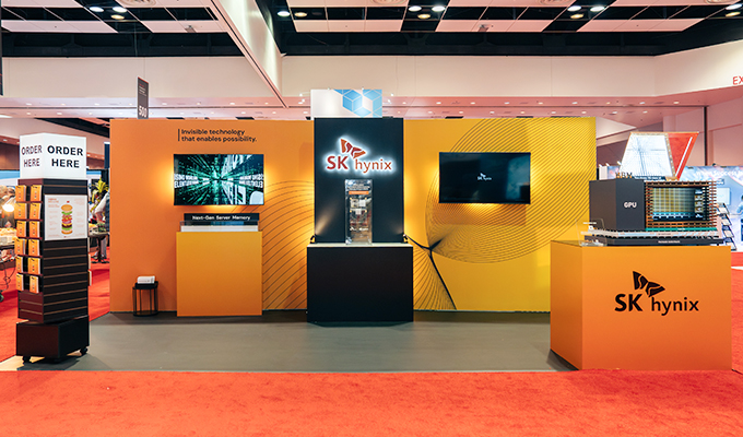
SK hynix’s booth at the TSMC OIP Ecosystem Forum 2024
Innovation in Focus: Leading HBM, AI & Data Center Products at the Booth
Situated next to the main TSMC booth, the SK hynix booth featured two main sections which showcased the company’s global No. 1 HBM and AI/data center solutions, respectively.
The HBM section featured the company’s industry-leading HBM3E. Boasting rapid processing speeds, high capacity, and outstanding heat dissipation, HBM3E is optimized for AI applications. This section not only highlighted the technological achievements of SK hynix, but also illustrated the strategic importance of its collaboration with TSMC to push the boundaries of AI innovation. Moreover, SK hynix’s HBM leadership was further underlined by the company’s recent announcement that it had become the first in the industry to begin volume production of the 12-layer HBM3E.
In the AI and data center solutions section, SK hynix presented the industry’s first 16Gb DDR5 product built using the 1c node, the sixth generation of the 10 nm process. Compared to the previous generation, the new product offers 11% faster operating speeds of 8 gigabits per second (Gbps) and 9% greater power efficiency to help data centers cut electricity costs. Marking a significant advancement in DRAM scaling, the 1cnm technology is set to be applied to other SK hynix products in the future.
This section also featured other key products in SK hynix’s portfolio, including DDR5 MCR DIMM3, DDR5 3DS RDIMM4, LPCAMM25, GDDR76, and LPDDR5T7. Each solution reflects significant advancements in AI memory technology, catering to diverse needs from high-performance computing (HPC) to mobile and graphics-intensive applications.
3Multiplexer Combined Ranks Dual In-line Memory Module (MCR DIMM): A module product with multiple DRAMs bonded to a motherboard in which two ranks—basic information processing units—operate simultaneously, resulting in improved speed.
43D Stacked Memory Registered Dual In-line Memory Module (3DS RDIMM): A high-density memory module used in servers and other applications to vertically connect DRAM dies through TSV, reducing module package height and boosting data transfer speeds.
5Low Power Compression Attached Memory Module 2 (LPCAMM2): LPDDR5X-based module solution that offers power efficiency and high performance as well as space savings. It offers performance levels equivalent to two DDR5 SODIMMs, making it optimized for on-device AI.
6Graphics DDR (GDDR): A standard specification of graphics DRAM defined by the Joint Electron Device Engineering Council (JEDEC) and specialized for processing graphics more quickly. It is now one of the most popular memory chips for AI and big data applications.
7Low Power Double Data Rate 5 Turbo (LPDDR5T): Low-power DRAM for mobile devices, including smartphones and tablets, aimed at minimizing power consumption and featuring low voltage operation. LPDDR5T is an upgraded product of the 7th generation LPDDR5X and will be succeeded by the 8th generation LPDDR6.
Other products on display included DDR5 MCR DIMM, DDR5 3DS RDIMM, LPCAMM2, LPDDR5T, and GDDR7
Presentation on 2.5D SiP Study for Enhancing HBM Quality & Reliability
During the forum, SK hynix’s Byoungdo Lee, Technical Leader of HBM PKG TE, gave a talk titled “A Collaborative Study on 2.5D System-in-Packages for Better Quality and Reliability of HBM.” Having encountered limitations using a proxy package to accurately recreate SiP8 conditions for the study, SK hynix opted to conduct open collaboration with companies including TSMC. This collaboration included preliminary evaluations as well as thermal and mechanical simulations at the SiP level. The study found that HBM products with SK hynix’s MR-MUF9 technology offer greater quality and reliability, and are ultimately able to overcome stacking limitations.
Additionally, the presentation covered three main advancements for HBM4, the upcoming sixth generation of HBM. Lee addressed the use of base logic die wafers10 to improve performance and power efficiency, as well as the development of 16-layer HBM utilizing Advanced MR-MUF or hybrid bonding11 packaging technology to meet demand for higher density products. Lastly, Lee spoke about planned SiP-level verification developments which aim to mitigate risks associated with the increased total product thickness.
8System-in-Package (SiP): A method of stacking and connecting multiple semiconductor chips in a single package to improve performance and efficiency, enabling advanced functions like high-speed data processing.
9Mass reflow-molded underfill (MR-MUF): A technology that ensures secure and reliable connections in densely stacked chip assemblies by melting the bumps between stacked chips.
10Base logic die wafer: A foundational semiconductor layer that contains the memory controller and logic circuitry, enabling high-speed communication between the stacked memory dies and the system.
11Hybrid bonding: A technology that stacks two or more chips atop one another in the same package, enabling high-density interconnections crucial for advanced HBM products.

SK hynix’s Byoungdo Lee presenting an OIP Partner Technical Talk on enhancing HBM
Strengthening AI Memory Leadership & Strategic Partnerships
At the TSMC OIP Ecosystem Forum 2024, SK hynix underlined its AI memory leadership and strengthened key industry partnerships. By showcasing key products such as the industry-leading HBM3E and the world’s first 1cnm DDR5 product, the company emphasized its ability to break technological boundaries. Looking ahead, the company is set to continue advancing its portfolio through collaboration with global partners to meet the growing needs of the AI era.


