In its quest to become a full stack AI memory provider, SK hynix continues to drive innovation and strengthen its competitiveness not only in DRAM but also in the NAND flash sector. For NAND flash products, the storage capacity depends on the number of stacked cell1 layers. Therefore, increasing the number of these layers is key to gaining a competitive edge.
1Cell: The smallest unit of data storage in a semiconductor.
This fourth installment of the One-Team Spirit series takes a closer look at SK hynix’s development of the world’s highest 321-layer NAND flash, known as the miracle of 321 layers, and spotlights the “one-team” spirit that made it possible.
Developing the 321-Layer 4D NAND Flash With Ultra-High Density and Capacity
The origins of SK hynix’s flash memory date back approximately 25 years. In the late 1990s, the company succeeded in developing 8-megabit (Mb) NOR flash2 products and focused on advancing its technology through dedicated research into the early 2000s.
2NOR flash: A type of flash memory in which cells are connected in parallel, unlike NAND. It features fast read speeds, excellent data integrity, and is mainly used for specialized tasks requiring high reliability. Its drawbacks include difficulty in scaling to large capacities and slower write speeds.
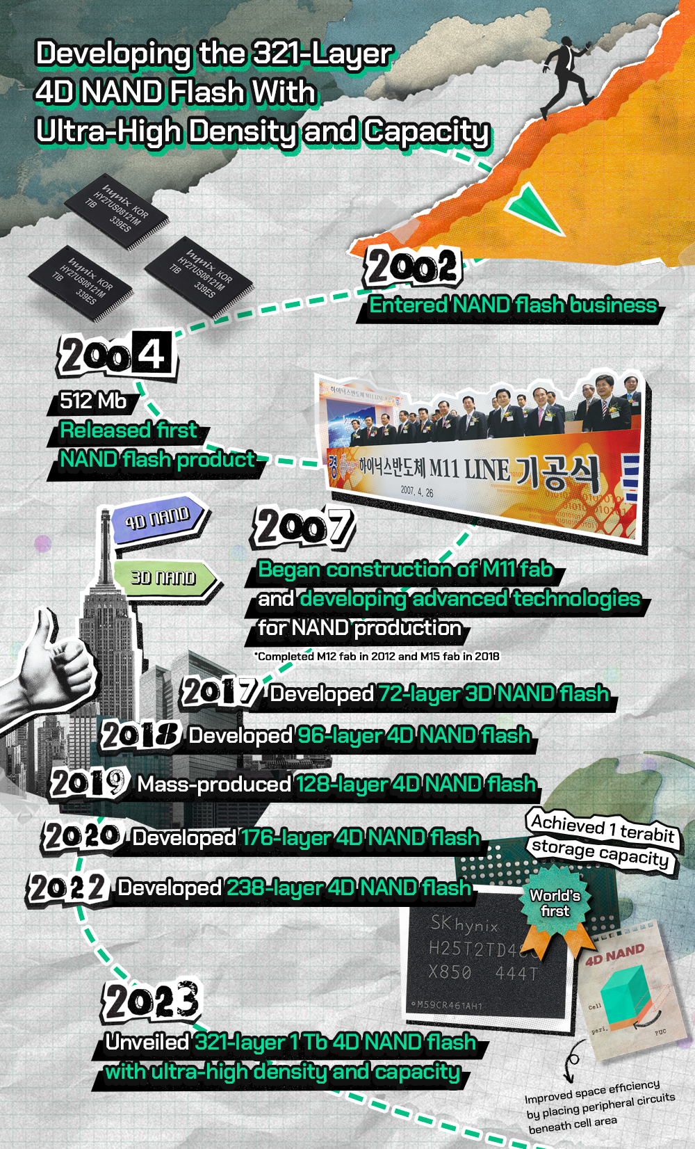
In 2002, as the market trend shifted toward NAND — which was better suited for high-capacity storage — SK hynix boldly changed the direction of its business. Though a latecomer to the NAND flash business, the company poured its efforts into research and entered the market in 2004 with its first 512 Mb NAND flash product. Within just three years, SK hynix had risen to third place globally in NAND flash revenue.
Following this, SK hynix accelerated the expansion of its NAND flash business and, in 2007, began construction of its M11 fab focused on NAND flash production. In the same year, the company developed a 24-layer multi-chip package (MCP) based on 16 Gb NAND flash followed by the 32 Gb NAND flash in 2008, steadily strengthening its technological capabilities and foundation.
Since the mid-2010s, the company has focused on developing 3D and 4D NAND flash technologies, in which cells are stacked vertically like apartments in a high-rise building. Compared to 2D technology, where cells are densely arranged on a flat plane, 3D NAND flash offers advantages in capacity, speed, and reliability. SK hynix advanced its technology in this field, developing the industry’s highest 72-layer 3D NAND flash in 2017, and in 2018 the company became the first in the world to develop 96-layer 4D NAND flash.
4D NAND flash technology further reduces the chip area by placing peripheral circuits beneath the cell array. To illustrate, it’s like converting an expansive outdoor parking lot into a multi-story underground parking lot to maximize space efficiency. By advancing this technology, SK hynix achieved stacking innovations with both 128-layer and 238-layer NAND flash. In 2023, the company introduced its 321-layer 1 terabit (Tb) 4D NAND flash which offers ultra-high density and capacity, and began full-scale mass production the following year. With this product, which densely houses hundreds of billions of cells on a chip no larger than a fingernail, SK hynix once again demonstrated its competitive edge in NAND flash technology.
From SLC to QLC: Completing the NAND Flash Lineup With One-Team Spirit
SK hynix’s NAND flash competitiveness is also highlighted through its advancement of cell storage technology. There are two main ways to increase NAND flash capacity: stacking cells higher and increasing the amount of information (bits) stored within a single cell. In other words, even with fewer layers, it is possible to develop high-capacity products if each cell can store more data.
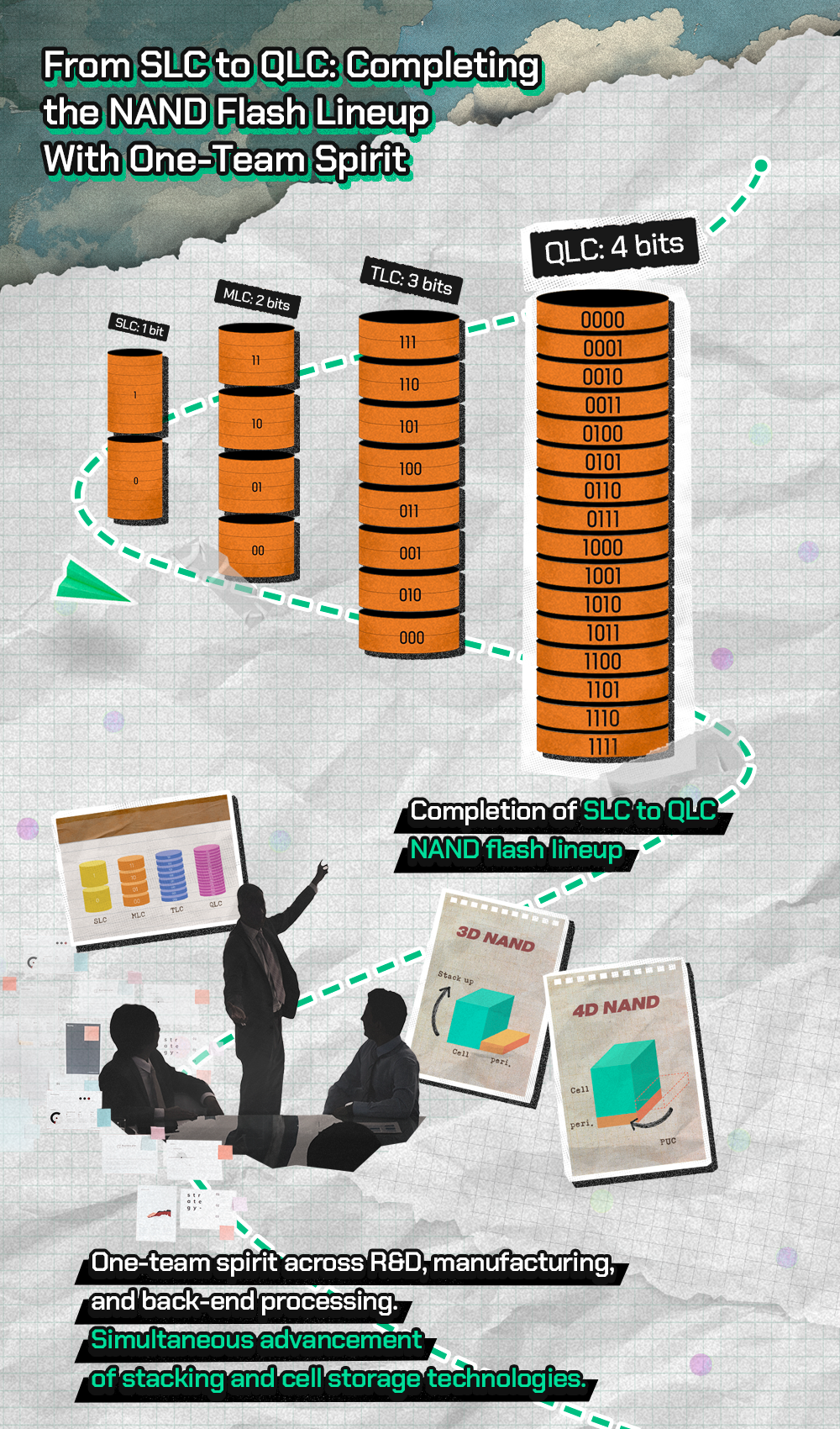
Therefore, SK hynix has progressively improved the efficiency of NAND flash cell structures by advancing from single-level cell (SLC), which stores 1 bit per cell to multi-level cell (MLC), triple-level cell (TLC), and quad-level cell (QLC).
The company’s key products include the 64 Gb MLC NAND flash released in 2013, the 256 Gb TLC 3D NAND flash introduced in 2017, and the 1 Tb QLC 4D NAND flash developed in 2019. By successfully developing the entire lineup from the high-speed SLC to the storage-efficient QLC, SK hynix has established a versatile portfolio capable of meeting diverse customer demands. At the core of these innovations was the one-team spirit that united the entire team. This united will was vital to solve the challenge of simultaneously advancing both cell stacking and cell capacity expansion technologies.
In recent years, the R&D team overcame technological limits by developing optimal devices and designing new 3D and 4D structures while at the same time integrating cell technologies such as TLC and QLC. Moreover, the manufacturing team developed precise process technologies to ensure the stable production of ultra-high-layer cell structures with enhanced reliability and storage performance. Finally, the back-end processing team secured packaging and testing technologies optimized for the new products, thereby improving quality at the final stage. As a result of this close inter-departmental collaboration, SK hynix was able to achieve the miracle of its 321-layer QLC NAND flash.
Beyond NAND Flash: Solution Innovation Driven by the One-Team Spirit
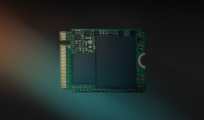
While NAND flash can be sold as a standalone product, it is also supplied as part of an integrated solution combined with software, firmware, and other components. To meet the needs of the AI and big data era, SK hynix is developing a range of NAND flash-based solutions including UFS3 and SSDs, built on its proprietary technologies.
3Universal Flash Storage (UFS): A storage specification for mobile devices characterized by high speed and low power consumption. In May 2025, SK hynix became the first in the world to develop version 4.1.
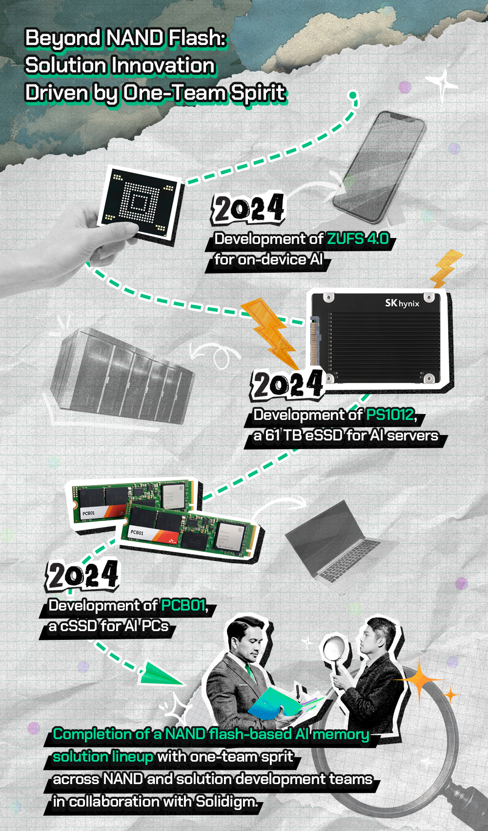
In particular, Zoned UFS (ZUFS) 4.0, developed by SK hynix in 2024, is a high-performance solution optimized for on-device AI environments. By leveraging zoned technology to group and manage data with similar characteristics in designated storage areas, it is recognized for improving both processing speed and efficiency.
SK hynix is also expanding its presence in the AI server and data center markets which require vast storage capacity. Having released the 61 TB QLC-based enterprise SSD (eSSD) PS1012 in 2024, the company is developing ultra-high-capacity solutions, including a 244 TB product using 321-layer 4D NAND flash and beyond. Also unveiled in 2024, the client SSD (cSSD) PCB01 for AI PCs is gaining attention as a high-performance storage solution that can accelerate on-device AI training and inference.
SK hynix has spent years building a comprehensive lineup of AI memory solutions that covers servers, data centers, and on-device applications. The driving force behind this innovation has been, once again, its one-team spirit. Securing solution capabilities requires extensive development collaboration across the chip and software areas. The NAND flash development team, which handles storage, must work closely with the solution development team, which develops firmware and software to control the chip. This must be further supported by the testing and optimization team based on the end-user environment. Collaboration with other companies, such as its affiliate Solidigm, also plays a key role in helping SK hynix take its capabilities to the next level.
SK hynix’s pursuit of technological advancement remains an ongoing journey. Through its one-team spirit, the company has demonstrated unique leadership with its 321-layer 4D NAND flash and the storage solutions built upon it. As it looks to become a full stack AI memory provider, SK hynix will continue to pioneer the future NAND flash market.