Hit enter to search or ESC to close
ENG
English
Chinese(中文)
Korean(한국어)
ENG
中文
KOR
Press Release
Business
Multimedia
Technology
Culture & People
ESG
Opinion
Fact Sheet
Earnings
아이콘
Sustainability Report
아이콘
PRESS CENTER
Press Release
Business
Multimedia
INSIGHT
Technology
Culture & People
ESG
Opinion
CORPORATE
Fact Sheet
Earnings
아이콘
Sustainability Report
아이콘
PRESS CENTER
INSIGHT
CORPORATE
Search
PRESS CENTER
PRESS CENTER
Press Release
Media Gallery
Event
INSIGHT
CORPORATE
MULTIMEDIA
INSIGHT
CORPORATE
MULTIMEDIA
Search Results "
Telegram老 号 出售➡️【SMMFS.COM】涨粉网站电报会员,AcK
"
VIEW ARTICLE
VIEW MULTIMEDIA
ALL
ALL
PRESS CENTER
INSIGHT
NEW
Newest
Oldest
Sorry, no results were found.
Please try again with different keywords.
Search
All
all
MEDIA GALLERY
image
video
infographic
video
[Tech Pathfinder] How SK hynix’s Advanced 4D NAND Technologies Are Overcoming Stacking Limitations
video
[Tech Pathfinder] How SK hynix’s Advanced 4D NAND Technologies Are Overcoming Stacking Limitations
video
[Tech Pathfinder] How SK hynix’s Advanced 4D NAND Technologies Are Overcoming Stacking Limitations
video
[Tech Pathfinder] How SK hynix’s Advanced 4D NAND Technologies Are Overcoming Stacking Limitations
infographic
[Tech Pathfinder] How SK hynix’s Advanced 4D NAND Technologies Are Overcoming Stacking Limitations
DOWNLOAD
infographic
3D Fe-NAND to Surpass 3D CTN Memory Following Cell Stacking Breakthrough
DOWNLOAD
infographic
3D Fe-NAND to Surpass 3D CTN Memory Following Cell Stacking Breakthrough
DOWNLOAD
infographic
3D Fe-NAND to Surpass 3D CTN Memory Following Cell Stacking Breakthrough
DOWNLOAD
infographic
[Tech Pathfinder] Small Size, Big Impact: Unveiling the Latest Advances in Semiconductor Packaging and Miniaturization
DOWNLOAD
infographic
[Tech Pathfinder] Small Size, Big Impact: Unveiling the Latest Advances in Semiconductor Packaging and Miniaturization
DOWNLOAD
infographic
[Tech Pathfinder] Small Size, Big Impact: Unveiling the Latest Advances in Semiconductor Packaging and Miniaturization
DOWNLOAD
infographic
[Tech Pathfinder] Small Size, Big Impact: Unveiling the Latest Advances in Semiconductor Packaging and Miniaturization
DOWNLOAD
infographic
How Innovative Convergence Technology Is Tackling DRAM Scaling Challenges
DOWNLOAD
infographic
How Innovative Convergence Technology Is Tackling DRAM Scaling Challenges
DOWNLOAD
infographic
How Innovative Convergence Technology Is Tackling DRAM Scaling Challenges
DOWNLOAD
image
Partnering to provide free GPS devices to track missing people
DOWNLOAD
video
Tenacity series 3. Hi-Gineers, their crisis tackling DNA
infographic
A look back on the past 10 years of SK hynix
DOWNLOAD
infographic
Classification of Semiconductor Packages
DOWNLOAD
infographic
Packaging Methods
DOWNLOAD
infographic
Fan in and Fan out Wafer Level Package
DOWNLOAD
infographic
SK hynix_Wafer stacking configuration
DOWNLOAD
infographic
SK hynix_Structure comparison of conventional sensor and stack sensor
DOWNLOAD
infographic
Three detailed porcesses of back grinding
DOWNLOAD
infographic
Changes in the number of semiconductor packaging pins (or balls) in contact with the system board
DOWNLOAD
infographic
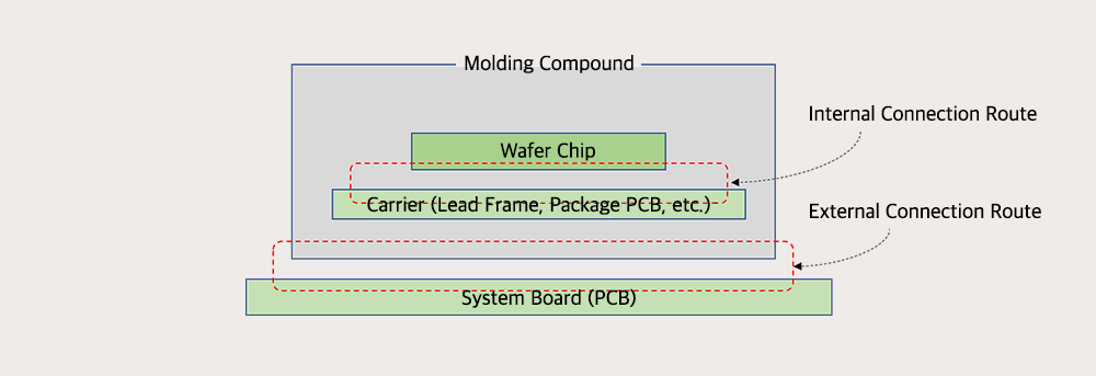
Internal and external structure of semiconductor package
DOWNLOAD
infographic
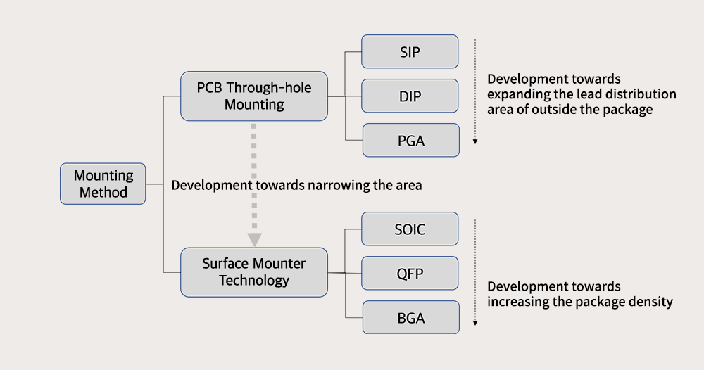
Diagram of package internal connection type, external connection type and mounting method
DOWNLOAD
infographic
3D Package with Via Hole penetrating silicon chips
DOWNLOAD
infographic
Types of external package type and mounting methods
DOWNLOAD
infographic
IC Package Types
DOWNLOAD
infographic
Latest 3-layer stacked image sensor
DOWNLOAD
infographic
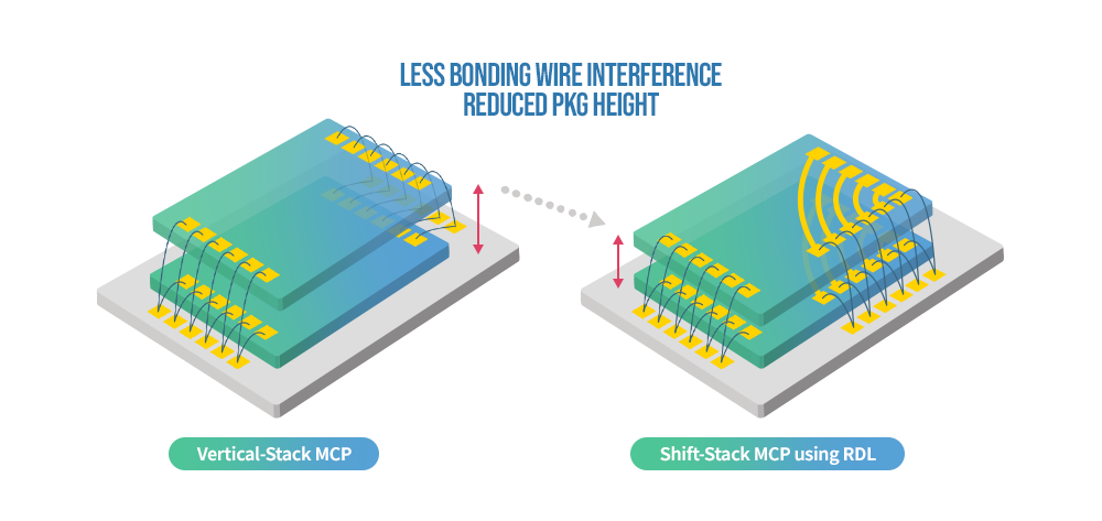
SK hynix_Two ways of Stack MCP
DOWNLOAD
infographic
SK hynix_Cross-Sectional View of Stack MCP
DOWNLOAD
infographic
3D TSV DRAM & Dual-Die Package
DOWNLOAD
infographic
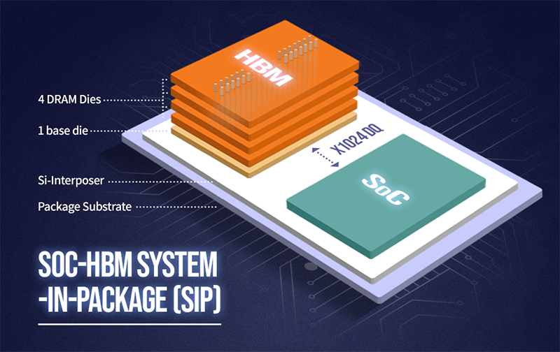
SoC-HBM System-in-Package (SiP)
DOWNLOAD
PRESS CENTER
PRESS CENTER
Press Release
Media Gallery
Event
INSIGHT
CORPORATE
MULTIMEDIA
INSIGHT
CORPORATE
MULTIMEDIA
![[Tech Pathfinder] How SK hynix’s Advanced 4D NAND Technologies Are Overcoming Stacking Limitations](https://img.youtube.com/vi/1GdlP7LBBHs/0.jpg)
![[Tech Pathfinder] How SK hynix’s Advanced 4D NAND Technologies Are Overcoming Stacking Limitations](https://img.youtube.com/vi/G6bI731f8_4/0.jpg)
![[Tech Pathfinder] How SK hynix’s Advanced 4D NAND Technologies Are Overcoming Stacking Limitations](https://img.youtube.com/vi/_FpA8xkCOYA/0.jpg)
![[Tech Pathfinder] How SK hynix’s Advanced 4D NAND Technologies Are Overcoming Stacking Limitations](https://img.youtube.com/vi/VjP_ntBeEUY/0.jpg)
![[Tech Pathfinder] How SK hynix’s Advanced 4D NAND Technologies Are Overcoming Stacking Limitations](https://d36ae2cxtn9mcr.cloudfront.net/wp-content/uploads/2023/12/14074455/SK-hynix_Pathfinder-EP.3_01.png)


![[Tech Pathfinder] Small Size, Big Impact: Unveiling the Latest Advances in Semiconductor Packaging and Miniaturization](https://d36ae2cxtn9mcr.cloudfront.net/wp-content/uploads/2023/07/25074116/SK-hynix_Pathfinder-ep2_MR-MUF.gif)
![[Tech Pathfinder] Small Size, Big Impact: Unveiling the Latest Advances in Semiconductor Packaging and Miniaturization](https://d36ae2cxtn9mcr.cloudfront.net/wp-content/uploads/2023/07/25074042/SK-hynix_Pathfinder-ep2_VFO.gif)
![[Tech Pathfinder] Small Size, Big Impact: Unveiling the Latest Advances in Semiconductor Packaging and Miniaturization](https://d36ae2cxtn9mcr.cloudfront.net/wp-content/uploads/2023/07/25073559/SK-hynix_Pathfinder-ep2_MCP.gif)
![[Tech Pathfinder] Small Size, Big Impact: Unveiling the Latest Advances in Semiconductor Packaging and Miniaturization](https://d36ae2cxtn9mcr.cloudfront.net/wp-content/uploads/2023/07/25073427/SK-hynix_Pathfinder-ep2_Chiplet.gif)