[Read the paper]
∙ Title: Co-packaged optics for high-performance computing and artificial intelligence
∙ Published in: Nature Electronics, 2026
∙ Authors: Seunghoon Hong (AI Infra Team Lead, SK hynix); Professor Kyusang Lee, Department of Electrical and Computer Engineering, University of Virginia (UVA); and researchers from the University of Illinois Urbana-Champaign (UIUC), Nanyang Technological University(NTU), the Massachusetts Institute of Technology (MIT) and Yonsei University
High Bandwidth Memory(HBM) has played a key role in enabling generative AI, significantly improving performance by overcoming memory bottlenecks within AI accelerator packages. However, as hyperscale AI clusters increasingly combine thousands of GPUs and HBM stacks, a new bottleneck has emerged: the bandwidth wall, which limits data movement between systems.
Against this backdrop, SK hynix and a team of global researchers have published “Co-packaged optics for high-performance computing and artificial intelligence“ in the Nature Electronics. The paper examines the development of CPO for HPC and AI, identifies the key technical challenges, and outlines a trajectory for the next-generation optical interconnect technology*.
Seunghoon Hong, SK hynix AI Infra Team Lead, and Professor Kyusang Lee of the Department of Electrical and Computer Engineering at the University of Virginia (UVA) served as corresponding authors*, leading a collaborative study with researchers from the University of Illinois Urbana-Champaign (UIUC), Nanyang Technological University (NTU), Massachusetts Institute of Technology (MIT), and Yonsei University.
On a wider level, the paper presents a comprehensive technology roadmap for how memory, advanced packaging, and optical compute interconnects (OCIs) should co-evolve to support next-generation AI systems. Crucially, it also demonstrates how SK hynix is moving beyond HBM innovation to help define the architecture of next-generation AI infrastructure at the system level.
From chips to systems: CPO is the key to scaling HBM innovation at the system level
Hyperscale AI models are no longer trained on a single chip or server. Instead, they run across massive networks organized into racks* and pods*. In these architectures, overall system performance depends not only on the connections between processors, memory, and AI accelerators, but also on how efficiently data moves between racks.
* Pod: A higher-level infrastructure unit that groups multiple racks together, enabling the integrated management of networking, power, and cooling
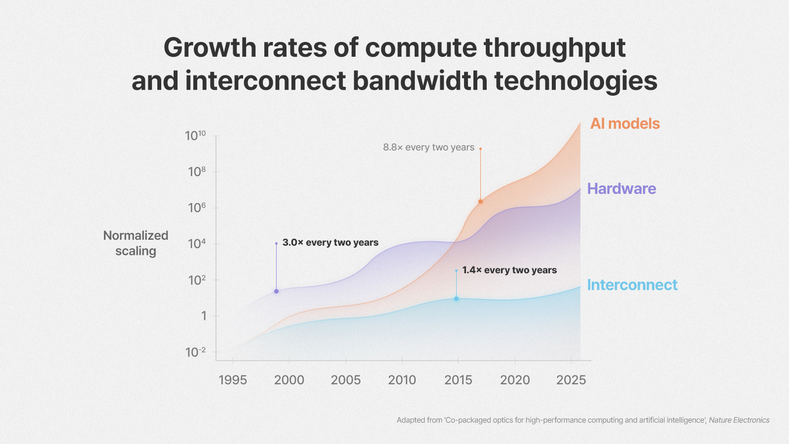
▲ Compute throughput has typically tripled every two years, while interconnect bandwidth has advanced only about 1.4-fold, creating a “bandwidth wall.”
In practice, compute throughput has tripled every two years, while interconnect bandwidth has only advanced 1.4-fold over the same period, making the bandwidth wall an increasingly significant challenge. Conventional copper-based electrical interconnects, which carry data beyond the chip package and between racks, suffer from rapidly increasing signal loss and power consumption as transmission distances grow. As a result, they are increasingly viewed as a limiting factor for next-generation AI data centers.
“Even if computing chips become more powerful, overall system performance cannot improve unless data movement between chips keeps pace,” said Professor Kyusang Lee. “Replacing copper interconnects, which face inherent physical limitations, with optical links is the most promising path toward future scalability.”
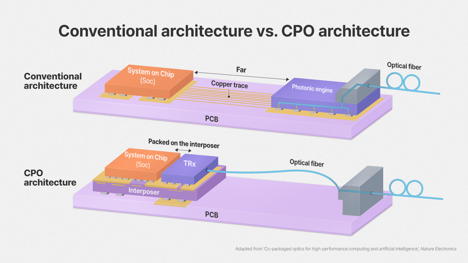
▲ CPO integrates optical engines ever closer to the processor. As the distance traveled by electrical signals is minimized, both bandwidth and energy efficiency improve.
With the bandwidth wall becoming an increasingly fundamental constraint on AI infrastructure, the paper positions CPO as central to overcoming this challenge. Seunghoon Hong, AI Infra Team Lead at SK hynix, describes the technology like this: “CPO integrates optical transceivers (TRx) into the same package as the processor, enabling chips to exchange data using light instead of long electrical interconnects. This fundamentally changes how data moves through AI systems, removing one of the biggest barriers to scaling compute.”
Conventional copper interconnects remain a cost-effective solution over short distances. As transmission speeds increase and communication distances grow, however, they require increasingly complex compensation circuitry, resulting in higher power consumption and greater data transmission latency. By integrating optical engines within the package, CPO minimizes the distance that high-speed electrical signals must travel and uses optical links for the remaining path. This extends high-speed communication across chips, racks, and pods while maintaining high bandwidth density, superior energy efficiency, and strong signal integrity with greater immunity to electromagnetic interference.
Based on this architecture, the researchers define clear technical targets for next-generation AI infrastructure, including more than 100 Tb/s of bandwidth per node, energy consumption below 1 pJ/bit, and chip-to-chip latency of less than 10 nanoseconds. The paper also presents a comprehensive technology roadmap outlining the evolution from 2D and 2.5D interposer-based configuration, as well as 3D heterogeneous stacking, together with the key technical challenges that must be addressed for commercial deployment.
Extending optical interconnects to memory for optimized data movement
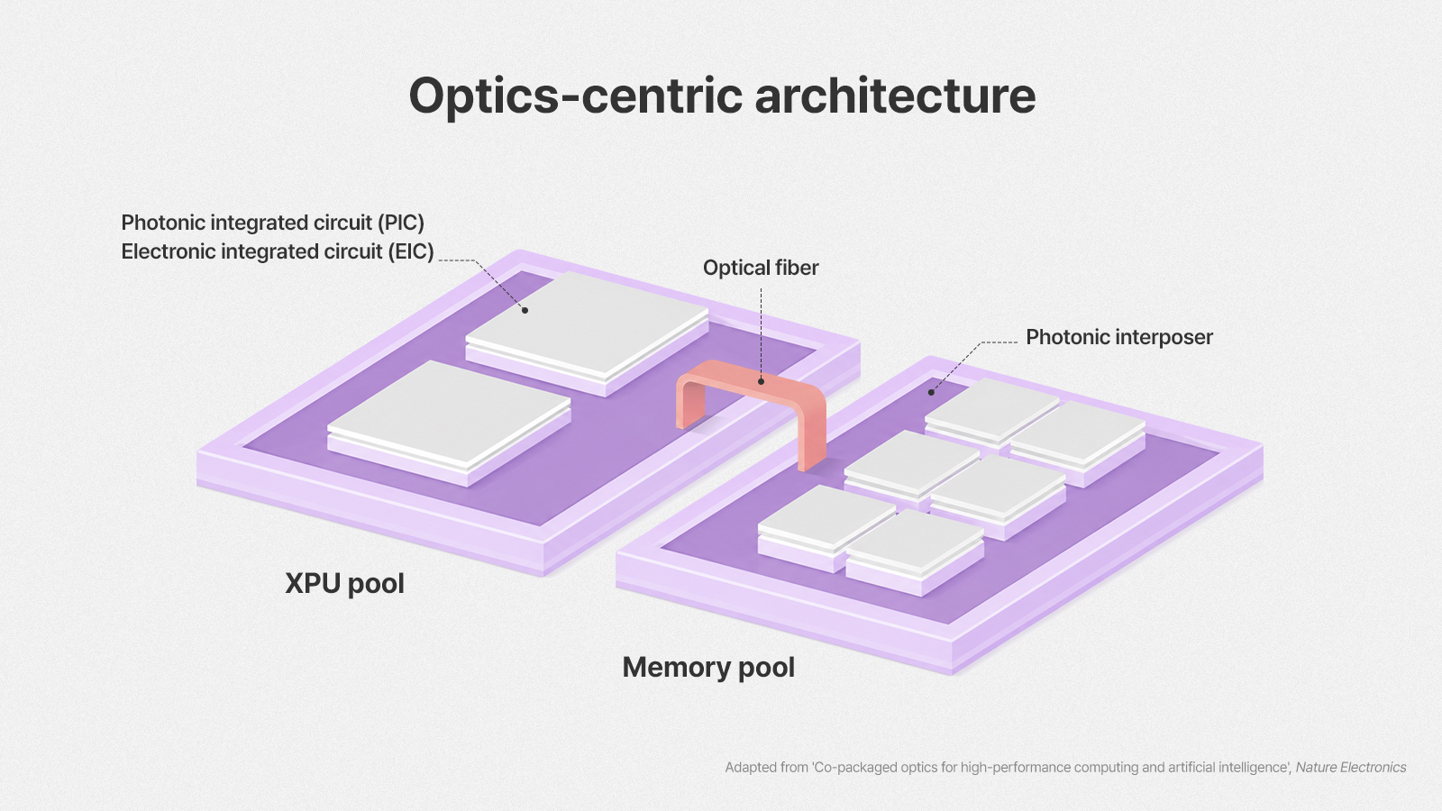
▲ Conceptual illustration of an optics-centric architecture in which a photonic interposer directly connects compute resources in the XPU pool with memory resources in the memory pool through optical links
In the long term, the evolution of CPO is expected to extend optical interconnects all the way to the memory interface. Moving beyond the physical constraints of conventional packaging, the proposed optics-centric architecture uses a photonic interposer to directly connect memory and processors, maximizing the efficiency of data movement across the system.
With this architecture, multiple AI accelerators can share a large memory pool, which enables more flexible system-level data movement while allowing AI infrastructure to scale more efficiently as models continue to grow.
“Optical interconnects are likely to become a foundational connectivity technology for future AI infrastructure,” said Professor Lee. “The technology has already moved beyond the laboratory and entered the early stages of commercialization. Significant challenges remain, from integrating low-power photonic devices to developing coherence protocols and improving system reliability. Ultimately, however, the key lies in co-designing memory devices and controllers, photonic components and packaging as a single integrated system. This is precisely where collaboration with SK hynix is especially meaningful.”
Hong added, “This collaboration is particularly significant because it brings together academic expertise and industry experience to present a shared vision for the future of AI infrastructure. We will continue to expand open collaboration that delivers tangible value to our customers and the broader AI ecosystem.”
INTERVIEW

Q1. Could you briefly introduce yourselves, including your primary research areas?
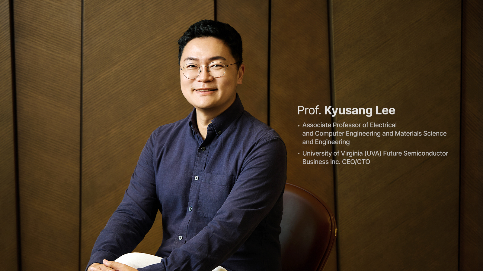
Professor Lee: I am a professor in the Department of Electrical and Computer Engineering at the University of Virginia (UVA). My research focuses on heterogeneous integration technologies, particularly the integration of ultrathin photonic and electronic devices within a single package for next-generation computing systems. Building on this research, I led the review presented in this paper, which provides a comprehensive overview of optical interconnects and CPO technologies for AI and HPC.
Hong: I began my career as a semiconductor engineer and have since gained experience across multiple areas of the memory business, including strategy and human resources. I currently lead long-term strategy for the memory industry in the AI era. My focus is on viewing memory not as a standalone component, but as part of the broader system architecture that drives our customers’ AI competitiveness. Through collaboration with partners across the industry, I work to create new value from a system-level perspective.
Q2. How do you feel about having your paper published in “Nature Electronics,” a prestigious scientific journal?
Professor Lee: It is especially meaningful to have achieved this milestone together with SK hynix, one of the world’s leading semiconductor companies. Rather than presenting the advancement of a single device, this paper offers a roadmap for the future of AI infrastructure. It is deeply rewarding to see the work resonate with both academia and industry. I hope it helps bring broader attention to the importance of this technology, and I would like to express my sincere gratitude to all of the researchers from the collaborating institutions who made this work possible.
Hong: We are very encouraged to have achieved this milestone through collaboration with leading researchers from around the world. The paper demonstrates the value of combining academic expertise with industry experience to present a shared vision for the future of AI infrastructure. SK hynix will continue working to deliver meaningful value to our customers and the broader industry ecosystem.
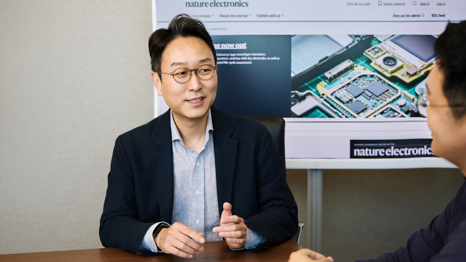
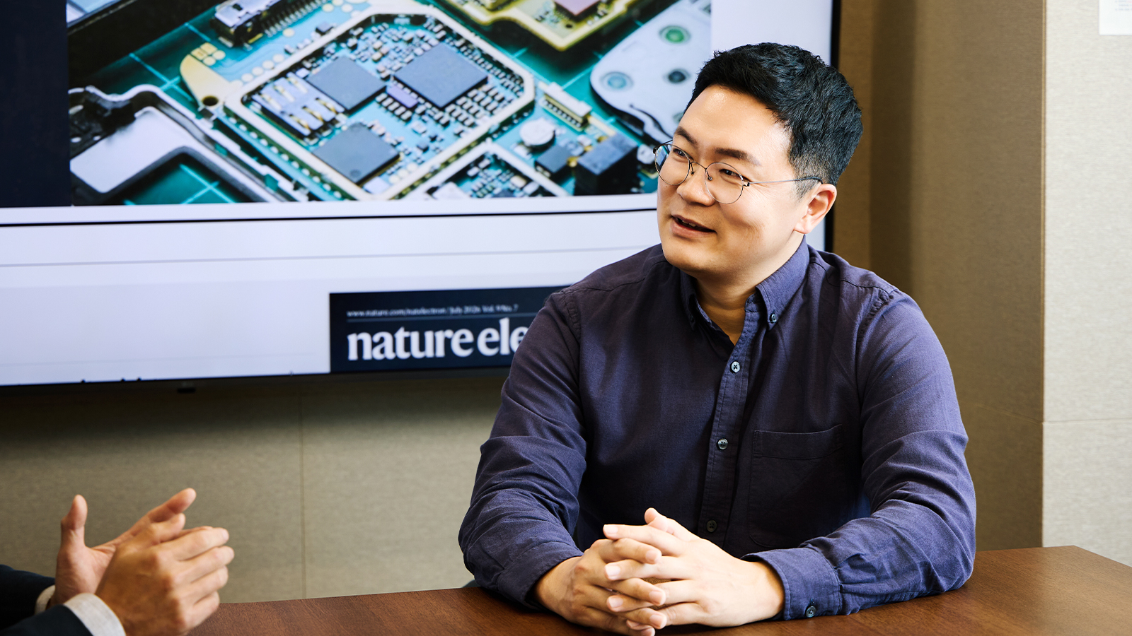
Q3. How did the collaboration between academia and industry strengthen this research?
Professor Lee: We gained a shared understanding of what it takes to transform a technology from something that is technically feasible into something that is commercially deployable. Academia excels at pushing the boundaries of performance, while industry understands the practical requirements for deploying technology at scale, including manufacturing yield, cost, cooling, and supply chain considerations. Bringing these perspectives together enabled us to develop a practical roadmap for the future of AI infrastructure.
Hong: When academia’s pursuit of next-generation technologies is combined with industry’s real-world experience, it enhances not only technical excellence but also the potential for commercialization. This collaboration reinforced our shared belief that industry-academia partnerships are a critical foundation for enabling customer success and driving innovation across the AI ecosystem.
Q4. The paper argues that optical connectivity should eventually extend to the memory interface. What advantages would this bring?
Professor Lee: Extending optical interconnects to the memory interface would overcome the physical constraints surrounding compute chips, removing limitations on both memory capacity and the number of electrical connections. It would also allow multiple AI accelerators to share a large memory pool, which would make AI infrastructure far more adaptable as AI models continue to grow in scale.
Hong: The greatest advantage is that it enables AI systems to scale more flexibly by improving data movement efficiency. Ultimately, this provides customers with a stronger foundation for operating AI infrastructure more efficiently.
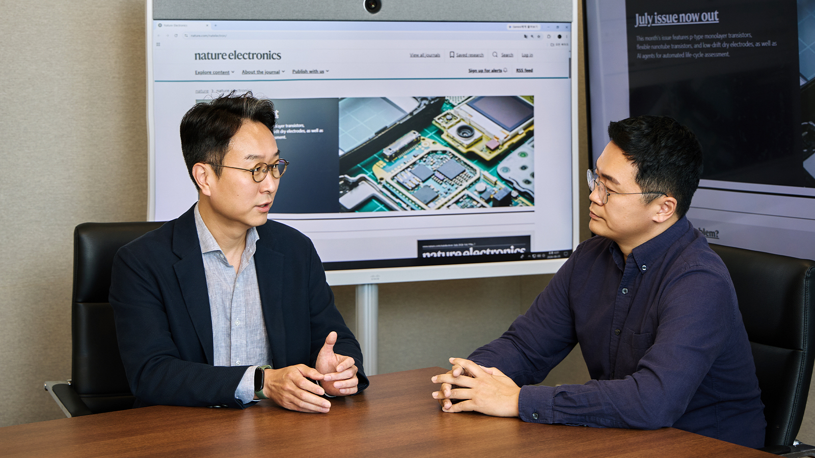
Q5. What will make CPO a key technology for future AI infrastructure, and where is your research headed next?
Professor Lee: CPO has the potential to become a foundational standard for future AI infrastructure because it offers four key advantages: high bandwidth density, excellent energy-distance efficiency, scalable parallel connectivity, and robust signal integrity with strong immunity to electromagnetic interference. We will continue working with industry partners to demonstrate pathways toward even greater energy efficiency through technologies such as ultrathin photonic material integration and massively parallel optical interconnects based on microLED (µLED) technology.
Hong: As customers continue to build larger AI systems, the importance of optical interconnects will only increase. Memory companies are evolving beyond the role of supplying individual components to becoming partners that help strengthen the competitiveness of customers’ entire systems through technologies such as CPO. Going forward, we will continue to expand open collaboration with customers and ecosystem partners to accelerate innovation across the AI infrastructure landscape.