AI doesn’t wait. The foundations of every industry are already cracking. This isn’t a story about one sector. Manufacturing. Finance. Healthcare. Data centers. The entire industrial order is being rebuilt around AI — and it’s happening now. Knowing about AI is no longer a competitive advantage. You need to see through it. That’s why our Newsroom is putting AI — and the semiconductors that power it — under the microscope.
In [Tech Note] Professor Seunghwan Joo of Inha University Manufacturing Innovation School discusses hybrid bonding.
Given the limits of performance improvement through chip scaling, chip stacking and connection methods have become key determinants of system power, speed, and thermal structure. In particular, semiconductors used in AI smartphones and AI servers require high bandwidth, creating an urgent need for new bonding technologies to replace existing bump* methods in 3D stacking structures, where inter-chip distances must be reduced to extremely short lengths to improve performance.
At the center of this change lies Hybrid Bonding*. This technology is gaining prominence as a future technology that will define the performance and structure of next-generation memory, HBM*, NAND flash (hereinafter NAND), 3D stacked DRAM, and AI accelerators.
* Hybrid bonding: A technology that directly connects chips without bumps when stacking. This allows the overall chip thickness to be reduced, enabling higher-layer stacking, and is considered a necessary technology for 16-layer and higher HBM products.
* HBM (High Bandwidth Memory): A high-value, high-performance memory product which vertically interconnects multiple DRAM chips and dramatically increases data processing speed in comparison to conventional DRAM products. There are six generations of HBM, starting with the original HBM followed by HBM2, HBM2E, HBM3, HBM3E, and HBM4.
Bump-less Chip Connections Enable High Efficiency and Bandwidth, Drawing Particular Attention in the HBM
Hybrid bonding is a next-generation chip connection technology that simultaneously bonds dielectrics* and metal (copper*). The name “hybrid” reflects the combination of these two bonding mechanisms. It is characterized by the elimination of conventional bumps and the direct bonding of copper to copper(Cu–Cu) to connect chips. This technology was developed to enhance performance by increasing connection density through decreased inter-chip spacing, thereby improving signal latency and thermal dissipation.
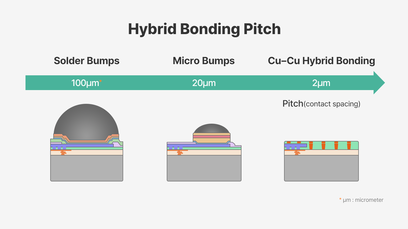
▲ Pitch Differences among Solder Bumps, Microbumps, and Hybrid Bonding
As shown in the figure, solder bumps have a pitch of about 100µm, while microbumps are approximately
20µm. In contrast, Cu–Cu hybrid bonding shrinks the pitch to below 1µm. As the pitch decreases, inter-chip distances narrow and connection paths become denser, offering a significant advantage for structures that require high bandwidth.
* Metal (Copper): Penetrating the dielectric layer and existing in an exposed form, copper serves as an ultra-high-density interconnect (I/O) that transmits electrical signals and power between chips.
Hybrid bonding was first commercialized in 2010, when it was applied to a CIS camera developed by Sony and used in the Apple iPhone 4. In 2019, YMTC adopted hybrid bonding in flash memory manufacturing, followed by product launches by Kioxia using the technology in 2023. SK hynix is reportedly also developing NAND products with more than 400 layers incorporating hybrid bonding by 2026, with mass production targeted for 2027. In the logic sector, AMD has already introduced the technology in its 3D V-Cache CPU product line. As such, hybrid bonding is already widely adopted across diverse fields—including logic, sensors, and mobile applications—and is expected to be adopted for HBM in the near future.
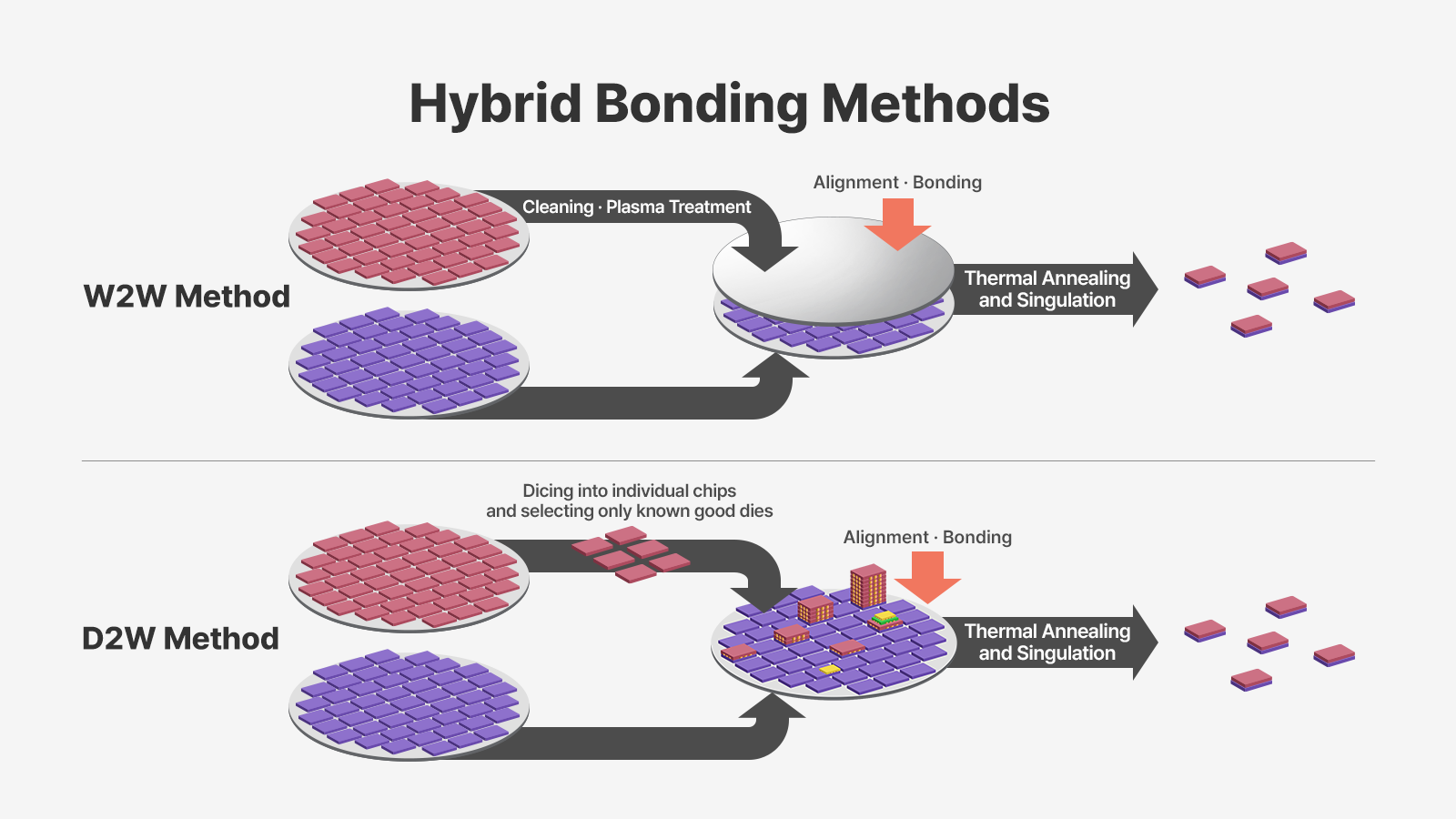
▲ Two Major Hybrid Bonding Methods
Hybrid bonding is broadly classified into two types: wafer-to-wafer(W2W), which bonds two wafers, and die*-to-wafer(D2W), which bonds a die and a wafer. W2W offers high productivity and is well suited for ultra-fine pitch applications because entire wafers are bonded at once; however, defective chips can negatively affect yield. D2W, on the other hand, achieves high yield and enables the integration of diverse chips by selectively bonding only KGD(Known Good Dies) to a wafer, but its production speed is slow because chips are processed one by one.
The W2W method has been commercialized and is currently in production for applications including Sony’s camera image sensors and flash memory, whereas the D2W method is exemplified by AMD’s 3D V-Cache. For HBM, the D2W approach is being adopted and is progressing toward commercialization.
The HBM sector is paying close attention to hybrid bonding because of the advantages this technology offers. In summary, these include ▲increased connection density ▲improved performance ▲reduced power consumption; lower thermal output and enhanced heat transfer efficiency ▲reduced height and ▲support for 3D packaging.
First, applying this technology narrows the contact spacing(pitch) between chips, significantly increasing connection density and enabling more data input/output (I/O) paths. Since signals travel the shortest distance, signal latency and losses are minimized, improving system performance and decreasing power consumption. In addition, the elimination of bumps and underfill* reduces chip height and thermal resistance. These changes provide a foundation for moving beyond 2.5D architectures—where memory and logic chips are connected on an interposer*—toward fully 3D HBM packaging. At the same time, an entirely new form of 3D HBM packaging is possible through hybrid bonding that enables direct chip-to-chip connections without through-silicon via (TSV*). Research on this approach is currently ongoing.
* Underfill: A material applied to fill the fine gaps between a chip(die) and the substrate during the packaging process.
* Interposer: An intermediate substrate used to connect multiple chips(e.g., CPUs, GPUs, and memory) within a single package.
* TSV(Through-Silicon Via): A technology that involves creating thousands of microholes in a DRAM chip to connect the upper and lower chip layers using vertically penetrating electrodes.
Hybrid Bonding: Emerging as a Foundational Technology Across the Entire Packaging Ecosystem, Alongside HBM
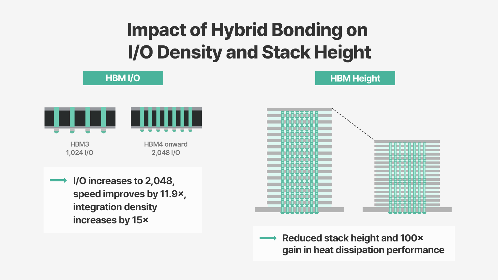
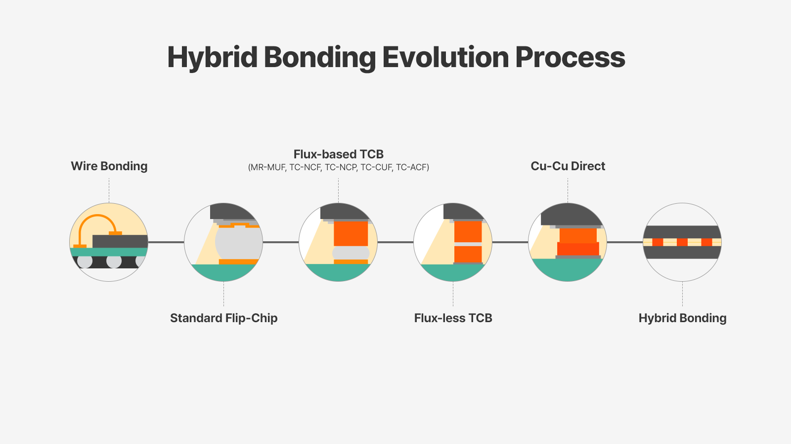
Hybrid bonding delivers significantly greater performance improvements than conventional TCB* technology. Speed increases by approximately 11.9 times, heat dissipation performance by over 100 times, and integration density by 15 times. For these reasons, hybrid bonding is being adopted in the manufacturing of most high-performance chip packaging. Just as wire bonding* was replaced by flip-chip* bonding in the past, TCB is expected to be increasingly replaced by hybrid bonding in the future.
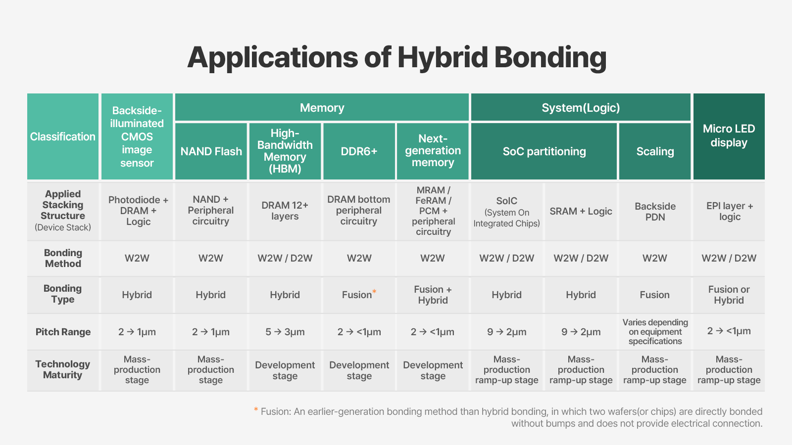
▲ Applications of Hybrid Bonding (Source: EV Group)
These changes are particularly evident in the Artificial Intelligence (AI) sector, where higher speed is required. Hybrid bonding has been applied to Intel’s AI server CPU, Clearwater Forest; AMD’s V-Cache CPUs and MI300 GPUs; and Apple’s M5 chips. Recently, CPO (Co-Packaged Optics) technology using hybrid bonding has also been adopted in network switches for ultra-high-speed communication in AI data centers, with Nvidia and Broadcom products being illustrative examples. This technology will be applied not only to next-generation HBM but also to DDR6+, Micro LED displays, Backside PDN*, and HBF*. As a result, hybrid bonding is expected to evolve into a fundamental technology enabling wafer-to-wafer connection in front-end processes across the entire packaging landscape.
* Wire Bonding: A method that connects semiconductor electrodes to a lead frame using fine gold or aluminum wires, thereby linking the chip to external circuits.
* Flip Chip: A method in which the circuit side of a semiconductor chip is flipped face-down and directly attached to a substrate using solder bumps.
* Backside PDN (Backside Power Delivery Network): A technology that places a semiconductor chip’s power delivery network on the backside of the chip.
* HBF (High Bandwidth Flash) Memory: A next-generation memory technology that significantly enhances speed and capacity by stacking multiple NAND flash dies.
▲ Impact of Hybrid bonding on I/O Density and Stack Height
Among the various application areas, HBM is the most promising. Current TCB methods are prone to deformation and stress caused by differences in the CTE (Coefficient of Thermal Expansion), making them unsuitable for pitches of approximately 7µm or below. In addition, heat dissipation becomes another major challenge when stacking 16 to 20 layers, as thermal accumulation intensifies.
Among TCB-based approaches, the MR-MUF (Mass Reflow–Molded Underfill) method is optimized for productivity and thermal dissipation, but still has limitations. In this process, DRAM dies are first connected using micro-bumps and stacked, after which liquid underfill material is injected to fill the gaps all at once and then cured. In contrast, hybrid bonding directly connects copper to copper within TSV instead of using microbumps, eliminating the need for underfill materials that occupy physical space. This not only minimizes the spacing between upper and lower DRAM layers but also removes microbump-related resistance, leading to faster signal transmission and more efficient thermal management.
From HBM4 onward, the number of I/Os is projected to double from 1,024 in HBM3E to 2,048, while the number of stacked layers is expected to increase to 16 to 20 or more. Under these conditions, conventional TCB—which uses epoxy resin for interlayer underfill—becomes impractical due to its limited heat dissipation capability compared with hybrid bonding, which directly connects copper to copper.
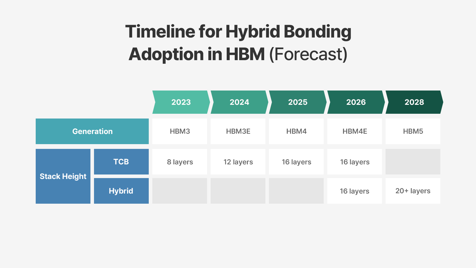
In addition, starting with HBM4, the package specification height increases from the current 720µm to 775µm. While existing packaging approaches remain viable up to HBM4, structural limitations are likely to emerge from HBM4E onward as minimizing DRAM spacing and improving thermal management become increasingly critical. Accordingly, next-generation HBM5 is expected to transition toward new packaging processes such as hybrid bonding.
Hybrid Bonding Powers AI Advancement — HBM Adoption Still “In Progress”
Products incorporating hybrid bonding are expected to play a key role in the development of AI technologies and the broader AI industry.
Currently, the AI sector requires three capabilities: higher speed, greater integration density, and smaller size. Reducing energy consumption by delivering these capabilities is the key, and hybrid bonding is a promising technology for achieving this. As mentioned earlier, applying hybrid bonding to GPU products that demand high performance improves computing speed by 11.9 times compared with conventional approaches. When applied to HBM products, it enhances heat dissipation performance by more than 100 times and increases integration density by over 15 times. Expectations are particularly strong in the AI memory segment, including HBM.
▲ Evolution Path to Hybrid Bonding
However, securing the technology does not necessarily lead to immediate adoption. The timing of HBM adoption is expected to be influenced by multiple factors, including manufacturing costs that are two to three times higher than those of flip-chip packaging, the maturity of process technology, and the pace of equipment development. There is also a significant gap in equipment capabilities between domestic and overseas suppliers. While overseas manufacturers have already completed equipment development and have begun applying it in production, domestic development remains in progress. Currently, Inha University’s laboratory, led by the author, is conducting a government-funded joint project in collaboration with a major company. Although the current equipment precision is approximately 100㎚ (nanometers), the research team plans to develop equipment capable of achieving 50nm and 25nm precision in the future, enabling applications for both HBM and logic devices.
▲ Predicted Timeline for HBM Adoption
Under these circumstances, the memory industry is likely to pursue a phased transition toward hybrid bonding while maximizing the use of TCB technology. At present, a flux*-free variant of TCB is being adopted, and further attempts are expected to directly connect copper to copper using TCB-based processes. When no viable alternatives remain, the industry will shift toward hybrid bonding. As such, reaching technological limits will inevitably accelerate the move to hybrid bonding. In the HBM segment, the full-scale adoption of hybrid bonding is most likely to occur in HBM4E or HBM5, where stack heights are projected to exceed 20 layers.
The timing of hybrid bonding adoption in HBM remains uncertain due to several practical constraints. However, it is clear that this technology represents the most viable solution for driving AI advancement and overcoming the physical limitations of conventional technologies. As a result, hybrid bonding is expected to establish itself as a mainstream platform across the entire semiconductor packaging sector and ultimately become a new standard for future semiconductor architectures.