There are countless technological achievements that paved the way for SK hynix’s success today, but one of the most remarkable is its advancement of miniaturization. The company’s ability to create microscopic circuits invisible to the naked eye has propelled it to the top of the global semiconductor industry. At the core of this success lies its deeply rooted ‘one-team’ spirit.
This latest episode of the One-Team Spirit series looks at SK hynix’s cutting-edge miniaturization capabilities and the defining moments when the company’s united culture fueled DRAM innovation.
Miniaturization: The Core of Innovation
Miniaturization, the process of scaling down circuits, has long been considered a necessity for technological innovation in the semiconductor industry and remains a key competitive advantage to this day.
The process is crucial as it significantly impacts both semiconductor performance and production efficiency. As semiconductor chips become smaller, more chips can be produced from a single wafer. Miniaturization also increases the number of transistors on a single chip, boosting the processing power per unit area. Furthermore, scaling transistors and devices leads to a reduction in a chip’s energy consumption and heat generation.
Enabling enhanced processing speed, energy efficiency and product reliability, SK hynix’s miniaturization technology is setting new global benchmarks thanks to its one-team spirit.

Breaking Through Technological Limits
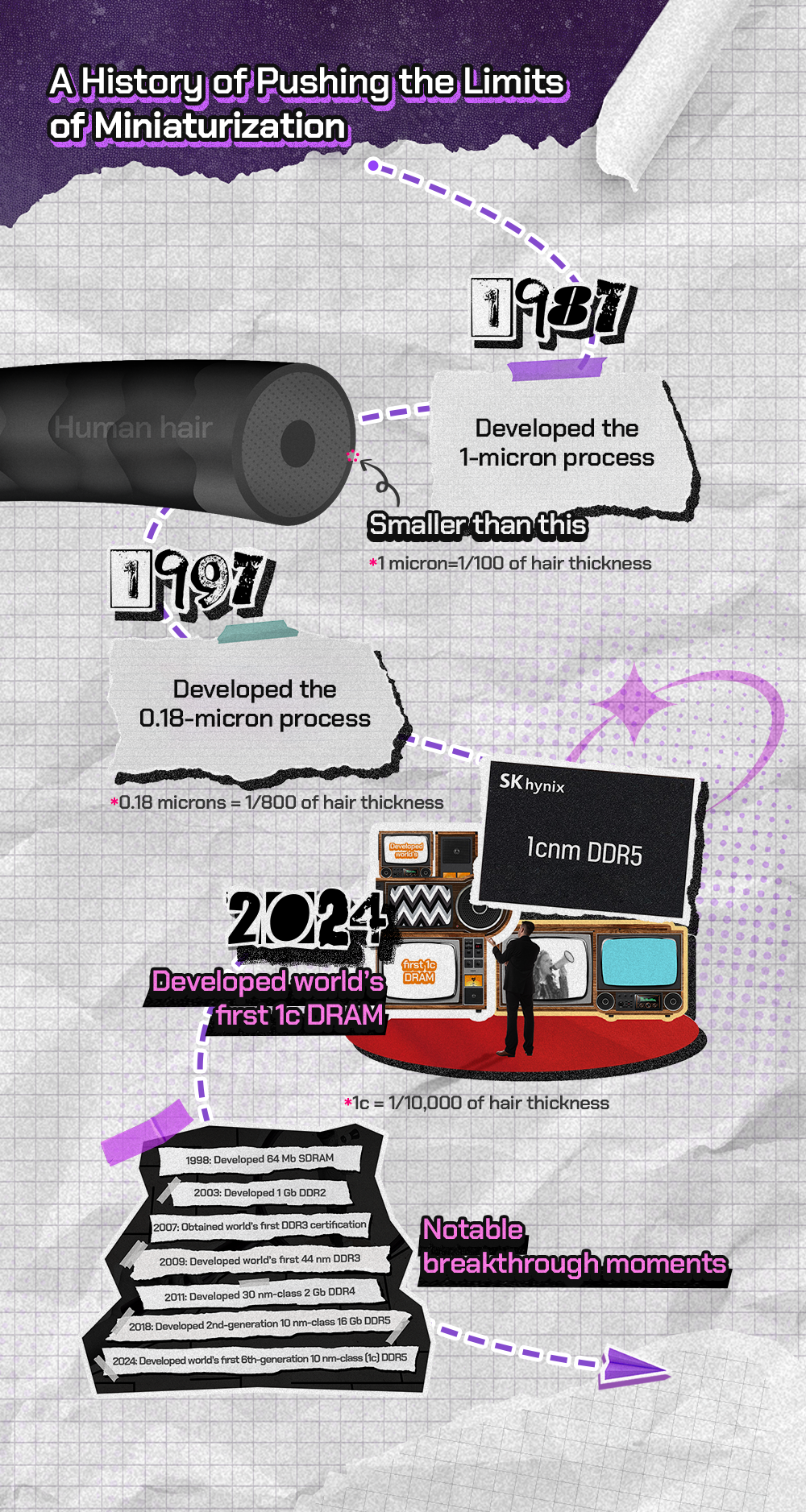
Historically, SK hynix has strived to break technological limits in miniaturization technology. Entering the semiconductor industry as a latecomer in 1983, the company made its mark in just four years as it successfully developed a then-groundbreaking 1-micron1 process, measuring just 1/100th the thickness of a human hair, in 1987.
1Micron (μm): A unit of length, equal to one millionth of a meter. Lower levels indicate higher refinement.
The company continued to strengthen its R&D efforts and investment, successfully introducing its advanced 0.18-micron process — roughly 1/800th the thickness of a human hair — amid the 1997 Asian financial crisis.
Incremental improvements in miniaturization reached the nanometer (nm) scale, measuring just one-billionth of a meter, in the 2000s. SK hynix continued to advance its miniaturization technology over the years by reducing circuit line widths, reaching the 60 nm class in 2006, the 40 nm level in 2009, and the 30 nm class in 2010. By 2012, the company had scaled down to the 20 nm range and reached the 10 nm class in 2018.
While Moore’s Law, which predicted that the number of transistors on a chip would double every two years through miniaturization, had been a guiding principle in the industry, concerns began to mount that semiconductor innovation was nearing its limit. Defying these concerns, SK hynix became the first in the world to develop the sixth-generation 10 nm-class DRAM process technology, known as 1c2 , in 2024. As an early 10 nm-class technology, this breakthrough enabled the development of circuits 10,000 times thinner than a human hair, delivering an 11% increase in speed and a 9% improvement in power efficiency compared to the previous generation, 1b.
21c: The sixth generation of the 10 nm DRAM process technology, which was developed in the order of 1x-1y-1z-1a-1b-1c.
What makes the development of the 1c DRAM process even more impressive is that it marks a critical juncture where technological complexity rises sharply. The challenges extend far beyond simply patterning finer circuits as issues such as atomic-scale physical limitations, unpredictable electron behavior, and signal interference emerge at this level. To overcome these obstacles, SK hynix embraced extreme ultraviolet (EUV) lithography, which enables more precise patterning thanks to its shorter light wavelength. This breakthrough significantly enhanced pattern accuracy and led to the successful development of 1c technology, pushing the boundaries of DRAM manufacturing.
SK hynix has also enhanced its Double Data Rate (DDR)3 technology over the years, resulting in improved DRAM speed. The company’s various DDR industry-firsts and landmarks are shown below.
3Double Data Rate (DDR): A comprehensive standard specification defined by the Joint Electron Device Engineering Council and applied to PCs, servers and other applications.
Key DDR Milestones
• September 1998: Mass-produced 64 megabit (Mb) DDR SDRAM chip
• August 2003: Developed world’s first 1 gigabit (Gb) DDR2
• May 2007: Obtained world’s first DDR3 certification
• February 2009: Developed world’s first 44 nm DDR3 DRAM
• April 2011: Developed 30 nm-class 2 Gb DDR4 DRAM
• December 2013: Developed industry’s first 20 nm-class LPDDR4 DRAM
• November 2018: Developed second-generation 10 nm-class 16 Gb DDR5 DRAM
• August 2020: Launched world’s first DDR5 DRAM
Behind each of these achievements lies SK hynix’s one-team spirit, which drove the team forward to overcome any technological challenges.
Historical Achievements Through Seamless Collaboration
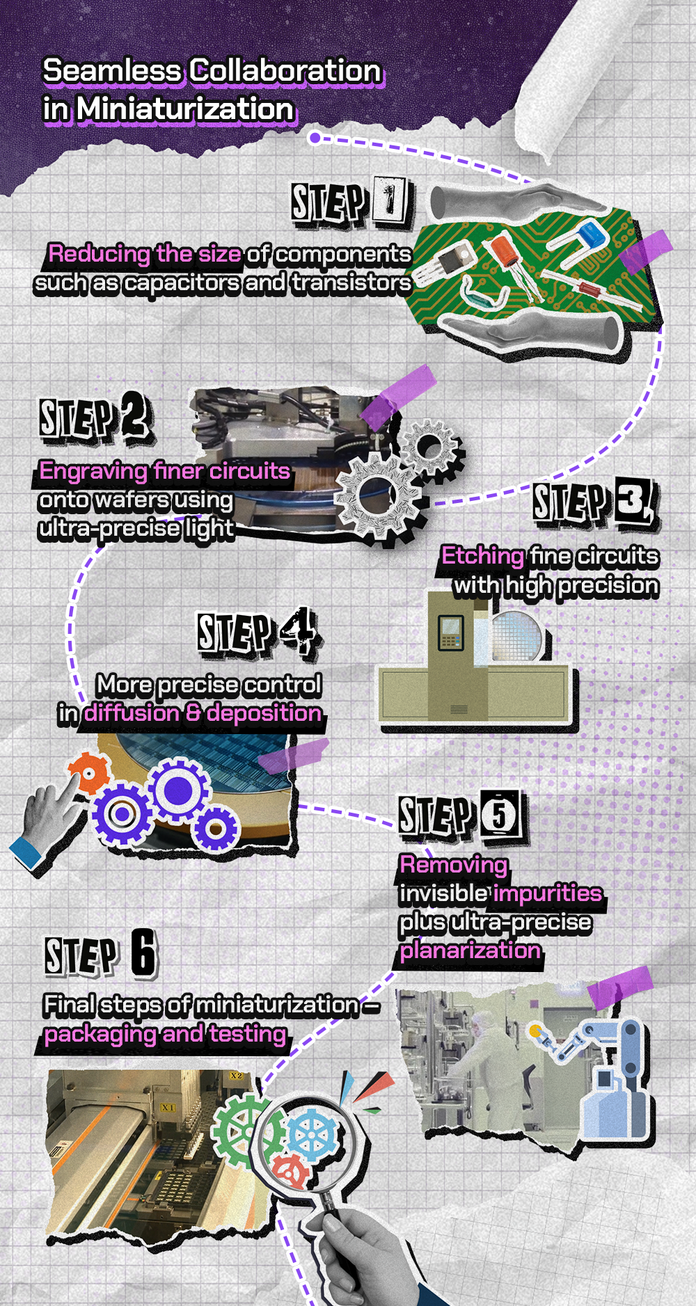
Miniaturization technology cannot be developed by an individual or a single team, but rather through a collective effort. To integrate billions of components such as capacitors and transistors into a chip the size of a fingernail and ensure they all function flawlessly, experts from across disciplines must work together.
At SK hynix, the R&D department, together with teams overseeing DRAM product planning and development, plays a key role in pioneering and securing advanced miniaturization technologies. They rigorously research and review technologies, including the 1c process technology, years before they are released to the public.
Bringing technologies such as these to life requires a significant input from the manufacturing side as well. To develop smaller circuits, wafers must undergo the highly precise photolithography process that creates intricate patterns. With the adoption of EUV processes in recent years, even finer patterning has become possible, significantly increasing semiconductor density.
Etching is also a critical process as it selectively removes material from the wafer to create ultra-fine circuit patterns. As etching only leaves behind essential materials, even the slightest error is difficult to reverse, directly affecting product yield and quality.
Deposition, which involves coating thin films onto a wafer surface to modify its electrical characteristics, is another crucial process. Specifically, atomic layer deposition (ALD) is employed to precisely control thin film thickness at the atomic scale for ultra-fine circuit structures.
Other key processes include diffusion, which injects necessary materials such as ions into ultra-fine patterns with precise depth and placement, and planarization, which removes microscopic impurities and creates smooth, defect-free wafers. Finally, the package and test (P&T) process, which involves making inter-chip electrical connections, thermal control, and functional testing of samples to ensure smooth operation of new technologies, has been key to pushing the limits of miniaturization.
This whole process is repeated hundreds of times in an iterative cycle before a single product is brought to market. Throughout each stage, even a single mistake can determine the success or failure of the technology. Every department involved must therefore commit to near-perfect precision and real-time communication and collaboration. This unwavering one-team spirit across all departments and members is widely recognized as the key factor behind SK hynix’s world-first achievement in developing 1c technology.
SK hynix’s 1c DRAM process is poised to revolutionize memory technology by delivering enhanced performance, improved quality, and greater production efficiency compared to previous generations. Importantly, this breakthrough is expected to have a wide-reaching impact on the market, as it can be applied across all next-generation DRAM product lines. These include AI memory technologies such as HBM4 , server and data center modules, LPDDR5 for mobile devices, and GDDR6 for graphics processing.
4High Bandwidth Memory (HBM): A high-value, high-performance memory product that vertically interconnects multiple DRAM chips and dramatically increases data processing speed in comparison to conventional DRAM products.
5Low-Power Double Data Rate (LPDDR): Low-power DRAM for mobile devices, including smartphones and tablets, which aims to minimize power consumption and features low voltage operation.
6Graphics DDR (GDDR): A standard specification of graphics DRAM defined by the Joint Electron Device Engineering Council and specialized for processing graphics more quickly.
Not resting on its laurels, SK hynix is continuing its pursuit toward even finer miniaturization processes based on strong collaboration that brings all employees together as one team. Building on this foundation, the company plans to strengthen its DRAM leadership and build a reputation as the most trusted full stack AI memory provider.