Seoul, July 02, 2020
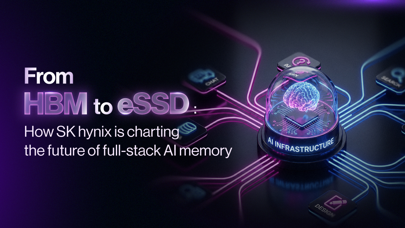
SK hynix Inc. (or ‘the Company,’ www.skhynix.com) announced that it has started the full-scale mass-production of high-speed DRAM, ‘HBM2E’, only ten months after the Company announced the development of the new product in August last year.
SK hynix’s HBM2E supports over 460GB (Gigabyte) per second with 1,024 I/Os (Inputs/Outputs) based on the 3.6Gbps (gigabits-per-second) speed performance per pin. It is the fastest DRAM solution in the industry, being able to transmit 124 FHD (full-HD) movies (3.7GB each) per second. The density is 16GB by vertically stacking eight 16Gb chips through TSV (Through Silicon Via) technology, and it is more than doubled from the previous generation (HBM2).
HBM2E boasts high-speed, high-capacity, and low-power characteristics; it is an optimal memory solution for the next-generation AI (Artificial Intelligence) systems including Deep Learning Accelerator and High-Performance Computing, which all require high-level computing performance. Furthermore, it is expected to be applied to the Exascale supercomputer – a high-performance computing system which can perform calculations a quintillion times per second – that will lead the research of next-generation basic and applied science, such as climate changes, bio-medics, and space exploration.
“SK hynix has been in the forefront of technology innovation that contributes to human civilization with achievements including the world’s first development of HBM products,” said Jonghoon Oh, Executive Vice President and Chief Marketing Officer (CMO) at SK hynix. “With the full-scale mass-production of HBM2E, we will continue to strengthen our presence in the premium memory market and lead the fourth industrial revolution.”
Annotation
■ HBM (High Bandwidth Memory)
– High performance, high bandwidth memory products that adopt TSV technology to dramatically accelerate data processing speed over traditional DRAMs.
■ TSV (Through Silicon Via)
– An interconnecting technology that connects the upper and lower chips through thousands of fine holes on DRAM chip.
– Delivers data, commands, and currents through column-shaped paths that penetrate the entire silicon wafer thickness after stacking multiple DRAM chips on the buffer chip.
– Up to 30% decrease in size and up to 50% decrease in power consumption over existing packaging methods.
■ Standards for data process speed conversion
– 1GB = 8Gb
– 3.6Gbps per pin with 1024 data I/Os (Inputs/Outputs) = 3686.4Gbps
– 3686.4Gbps / 8 = 460.8GB/s (Gb -> GB conversion)
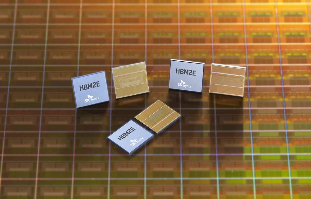
Figure 1. SK hynix starts mass-production of high-speed DRAM, ”HBM2E”

Figure 2. SK hynix employees posing for the commemorative photo celebrating the mass-production of HBM2E
About SK hynix Inc.
SK hynix Inc., headquartered in Korea, is the world’s top tier semiconductor supplier offering Dynamic Random Access Memory chips (“DRAM”), flash memory chips (“NAND flash”) and CMOS Image Sensors (“CIS”) for a wide range of distinguished customers globally. The Company’s shares are traded on the Korea Exchange, and the Global Depository shares are listed on the Luxemburg Stock Exchange. Further information about SK hynix is available at www.skhynix.com, news.skhynix.com.
Media Contact
SK hynix Inc.
Global Public Relations
Technical Leader
Jaehwan Kevin Kim
E-Mail: global_newsroom@skhynix.com
Technical Leader
Sejin Julia Yoo
E-Mail: global_newsroom@skhynix.com
Technical Leader
Eun Suk Yixi Lee
E-Mail: global_newsroom@skhynix.com