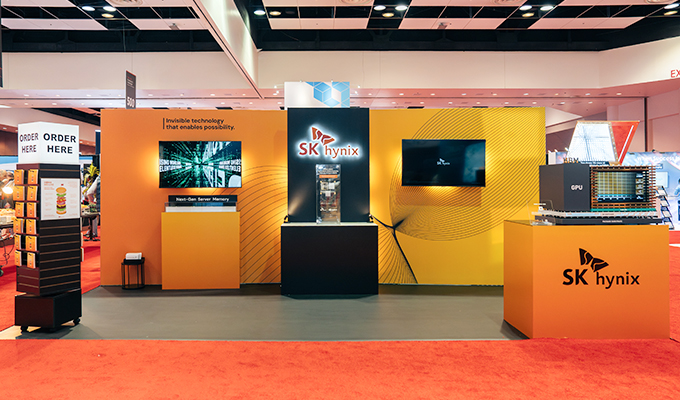
SK hynix showcased groundbreaking memory solutions including HBM41 at the TSMC 2025 North America Technology Symposium held in Santa Clara, California on April 23.
1High Bandwidth Memory (HBM): A high-value, high-performance product that vertically stacks multiple DRAM chips to dramatically enhance data processing speed compared to conventional DRAM. There are six generations of HBM, starting with the original HBM followed by HBM2, HBM2E, HBM3, HBM3E and HBM4.
The TSMC North America Technology Symposium is an annual event in which TSMC shares its latest technologies and products with global partners. This year, SK hynix participated under the slogan “Memory, Powering AI and Tomorrow,” highlighting its technological leadership in AI memory through exhibition zones including HBM Solutions and AI/Data Center Solutions.


SK hynix’s 12-layer HBM4 and 16-layer HBM3E on display alongside NVIDIA’s B100 GPU
In the HBM Solution section, SK hynix presented samples of its 12-layer HBM4 and 16-layer HBM3E products. The 12-layer HBM4 is a next-generation HBM capable of processing over 2 terabytes (TB) of data per second. In March, the company announced it has become the first in the world to supply HBM4 samples to major customers and plans to complete preparations for mass production within the second half of 2025.
The B100, NVIDIA’s latest Blackwell GPU equipped with the 8-layer HBM3E, was also exhibited in the section along with 3D models of key HBM technologies such as TSV2 and Advanced MR-MUF3, drawing significant attention from visitors.
2Through-Silicon Via (TSV): A technology to connect the upper and lower layers of DRAM chips by creating thousands of microscopic holes in each of the chip layers and running vertical electrodes through those openings.
3Advanced MR-MUF: A next-generation MR-MUF technology that incorporates warpage control, allowing chips which are 40% thinner than conventional chips to be stacked without warping. Additionally, the use of a new protective material improves heat dissipation.

In the AI/Data Center Solutions section, SK hynix displayed its lineup of server memory modules, including RDIMM4 and MRDIMM5 products. The section featured various high-performance server modules based on DDR5 DRAM built using the 1c node,6 the sixth generation of the 10 nm process technology.
4Registered Dual In-line Memory Module (RDIMM): A server memory module product in which multiple DRAM chips are mounted on a substrate.
5Multiplexer Combined Ranks Dual In-line Memory Module (MRDIMM): A server memory module product in which multiple DRAM chips are mounted on a substrate. Speed is enhanced by operating two ranks—the basic operating units of the module—simultaneously.
6Previous generations of the 10 nm DRAM process have been named using number-letter designations in the order of 1x, 1y, 1z, 1a and 1b. In August 2024, SK hynix became the first in the world to successfully develop the sixth generation of the process, named 1c.
Notably, SK hynix exhibited a range of modules designed to enhance AI and data center performance while reducing power consumption. These included the MRDIMM lineup with a speed of 12.8 gigabits per second (Gbps) and capacities of 64 GB, 96 GB, and 256 GB; RDIMM modules with a speed of 8 Gbps in 64 GB and 96 GB capacities; and a 256 GB 3DS7 RDIMM.
73D Stacked Memory (3DS): A high-bandwidth memory product in which two or more DRAM chips are packaged together and interconnected using TSV technology.


Visitors gather at SK hynix’s booth to see the latest memory innovations
At the TSMC 2025 North America Technology Symposium, SK hynix’s next-generation solutions such as HBM4 drew great attention from industry officials. By successfully mass-producing its HBM lineup through continued technological collaboration with partners such as TSMC, the company aims to expand the AI memory ecosystem and further solidify its industry leadership.