At the TSMC Technology Symposium 2026, held in the heart of Silicon Valley, SK hynix demonstrated its dominant standing as an AI memory powerhouse and reaffirmed its strong partnership with TSMC. In a keynote address, the company put forth the concept of ‘the integration of memory and logic’ and outlined a roadmap for the AI era. Here is a firsthand look at the event and its electric atmosphere.
A New Era Built on Semiconductors: Innovative Technologies Shared for AI Optimization


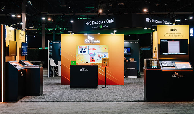
SK hynix booth at the TSMC Technology Symposium 2026
On the 22nd (local time), the Santa Clara Convention Center in San Jose, California, was packed with crowds from early morning. TSMC hosts its Open Innovation Platform (OIP) forums across seven major regions worldwide, bringing together semiconductor design and manufacturing partners to share the latest technologies and collaborative achievements. The North American symposium, held under the slogan “Expanding AI with Leadership Silicon,” showcased innovative technologies optimized for AI accelerators and High Performance Computing (HPC).
In the area of logic technology, the event focused on progress in advanced process nodes beyond 3㎚, spanning 2㎚, A16, and A141. In the packaging domain, TSMC highlighted stacking innovations leveraging technologies such as CoWoS2, InFO3, and SoIC4. Through these developments, TSMC set out a clear strategic direction to target the AI data center and cloud markets with high density transistors and low power architectures, keeping pace with the rapid expansion of AI solutions across domains ranging from HPC to smartphones and autonomous driving.
1A16 refers to TSMC’s next generation 1.6㎚ class process, while A14 denotes the subsequent 1.4㎚ class advanced process planned to follow A16.
2CoWoS (Chip on Wafer on Substrate): TSMC’s 2.5D packaging technology that places a chip on a wafer and then connects it to a substrate. By arranging logic chips and HBM side by side on a single package, it increases data transfer speeds and is considered a key enabler for AI accelerators and HPC.
3InFO (Integrated Fan-Out): A packaging approach that extends circuitry beyond the chip boundary using fan-out technology instead of a traditional package substrate. It reduces thickness while improving power efficiency, and is primarily used in mobile application processors.
4SoIC (System on Integrated Chips): An advanced 3D stacking packaging technology that vertically bonds different chips together. Utilizing hybrid bonding technology that connects chips without bumps, SoIC widens data processing bandwidth and reduces chip size, making it an essential technology for next generation AI semiconductor production.
The Way Forward in the AI Era: Disruptive Innovation That Breaks Down Boundaries
SK hynix Chief Development Officer (CDO) Ahn Hyun delivered a keynote address titled “The Next Era of AI Memory: Intelligent, Integrated, and Co-created,” making a compelling case for disruptive innovation that breaks down boundaries to overcome technological limits.
CDO Ahn began by outlining the direction of memory technology that SK hynix is pursuing in the AI era. “The most critical obstacle hindering the advancement of AI today is the Memory Wall, a bandwidth bottleneck that prevents the rapid processing of ever-growing volumes of data,” he noted. “To break through this barrier, we need efforts that go beyond incremental improvements to existing architectures and take a fundamentally new approach.”
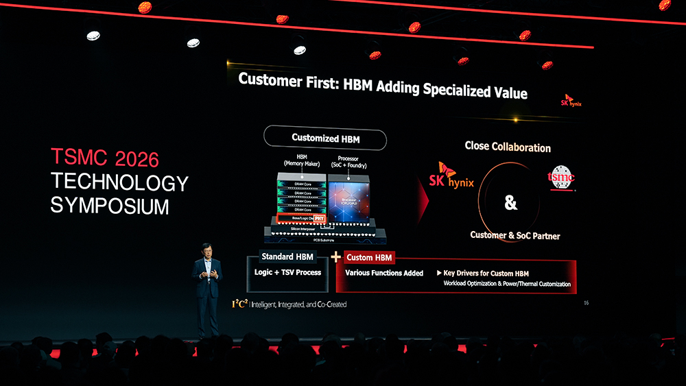
He further stated, “SK hynix is evolving from a simple ‘provider’ into a ‘creator’ that collaborates from the architecture design stage to devise and deliver the memory solutions that are needed.” He added, “Going forward, we will move beyond supplying standardized HBM for AI accelerators to offering custom HBM tailored to specific customer requirements, and we will extend this approach across all solutions spanning DRAM and NAND to enhance the performance and efficiency of AI systems.”
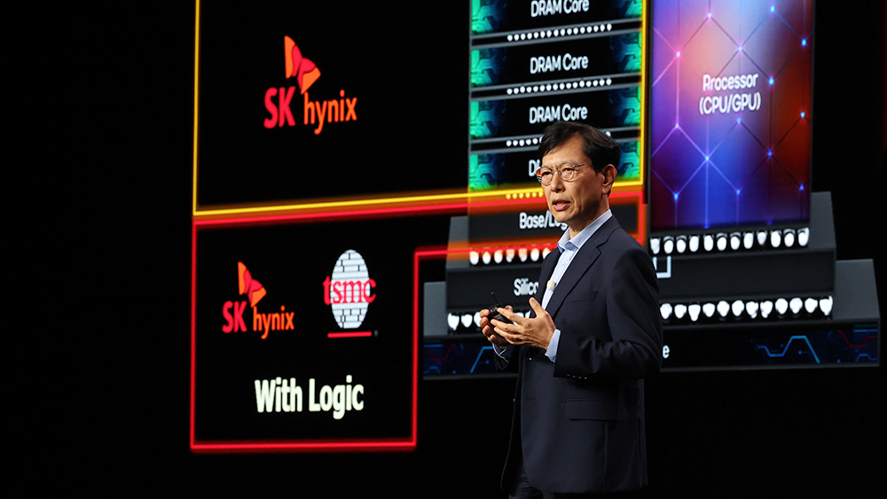
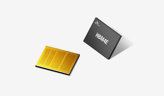
CDO Ahn also presented a new technological vision that SK hynix is preparing. “The integration of memory and logic technologies represents a new breakthrough that can transcend the limitations of existing architectures to maximize AI performance,” he said. “Building on this foundation, we will strengthen our strategic collaboration, including the adoption of TSMC’s advanced logic processes for the base die starting with HBM4, and provide a wide range of customized solutions optimized for diverse customer workloads, from custom HBM to HBF5 and 3D Stacked DRAM on Logic6.”
5HBF (High Bandwidth Flash): A next-generation NAND solution with enhanced ultra-high-speed data transfer capabilities, designed to efficiently handle the surge in large-scale computational data (such as KV Cache). Like HBM, it applies logic processes to the base die to maximize performance.
63D Stacked DRAM (3D Stacked DRAM on Logic): A state-of-the-art stacking technology that vertically stacks DRAM directly on top of logic semiconductors such as SoC (System on Chip). By significantly increasing data pathways (I/O), it minimizes latency and dramatically improves power efficiency and space utilization, making it particularly suited for on-device AI applications.
Finally, CDO Ahn defined ‘collaboration’ as the core value essential for the frontlines of AI, emphasizing SK hynix’s role as the optimal partner for the AI era. “SK hynix is the optimal partner with unrivaled technological capabilities in AI memory, including HBM,” he said. “Let us become ‘one team’ where all partners share technological progress in real time and solve complex problems together, and open a new AI era together.”
The Power of ‘Invisible Technology’ Opening New Possibilities for AI
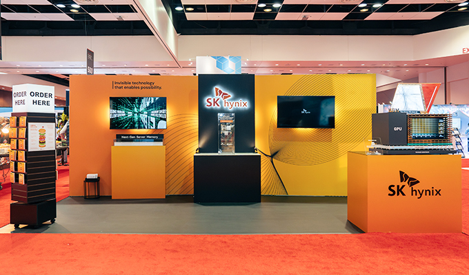
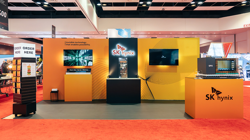
Alongside the symposium, SK hynix also participated in the concurrent exhibition, showcasing a wide array of advanced memory solutions. Under the concept of “Invisible Technology that Enables Possibility,” the company placed its key HBM7 product lineup front and center, focusing on demonstrating the critical role that SK hynix’s AI memory, invisible from the outside, plays inside products to enable AI.
7HBM (High Bandwidth Memory): A high-value, high-performance product that vertically connects multiple DRAM chips to increase capacity and dramatically improve data processing speed. HBM has evolved through successive generations: HBM, HBM2, HBM2E, HBM3, HBM3E, and HBM4.
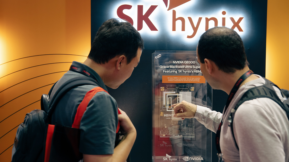
The HBM3E section drew the most attention at the exhibition. It presented the 12-layer HBM3E mounted inside NVIDIA’s GB300, broken down into three layers to provide a detailed, easy-to-understand explanation of the role HBM plays within actual products. Visitors were seen closely examining the product images displayed at each layer, and many engaged booth staff with questions, showing keen interest.


A 3D model showcasing the 16-layer 48GB HBM4 product and its enlarged internal structure
The HBM4 section, featuring the 16-layer 48GB HBM4 product and a 3D model illustrating its enlarged internal structure, also attracted significant interest. Notably, the product description included the phrase “Powered by base die in TSMC advanced logic,” underscoring the close technological partnership with TSMC.


SK hynix’s server DRAM product lineup
The company also showcased its latest server DRAM lineup, demonstrating its unmatched technology leadership. At the exhibition, SK hynix displayed the 256GB 3DS RDIMM8, which delivers the industry’s largest capacity; the 128GB MRDIMM9, optimized for high performance computing environments; and the 64GB RDIMM, the world’s first to apply the 1c-nanometer (1c㎚) process to maximize power efficiency. These products were presented side by side to highlight the company’s latest lineup targeting the server market. Additionally, the 192GB SOCAMM210 which also features the 1c㎚ process and drew considerable attention as a next generation solution designed specifically for AI servers, delivering low power consumption and high performance in a new form factor.
8RDIMM (Registered Dual In-line Memory Module): A server memory module composed of multiple DRAM chips.
9MRDIMM (Multiplexed Rank Dual In-line Memory Module): A memory module in which two ranks, the basic operating units of a module, operate simultaneously, significantly improving speed.
10SOCAMM (Small Outline Compression Attached Memory Module): An AI server optimized memory module based on low power DRAM.


HBM burger souvenirs and recipe cards presented by SK hynix at the event
The event activities held alongside the exhibition were also a hit with visitors. SK hynix handed out our company swags to visitors who followed its LinkedIn channel, featuring a ‘burger’ that creatively represented HBM’s intricate stacking structure. The company also distributed cards containing a ‘Stacking Recipe’ that broke down complex technical concepts in an accessible way, replacing the typical formality of a technology exhibition with a more approachable, friendly atmosphere.
SK hynix said, “Through this symposium, we were able to reaffirm our strong partnership with TSMC while broadly communicating the direction of SK hynix’s technological evolution.” The company added, “Moving forward, we will continue to solidify our position as a Full Stack AI Memory Creator, built on our unrivaled technology leadership, and lead the AI era together with our global partners.”