As AI technology advances, the memory semiconductor industry faces mounting challenges. Amid rising demands for performance, density, and reliability — and as technological limits become more pronounced — the solution lies in returning to semiconductor fundamentals: device technology.
This technological foundation also underpinned SK hynix’s performance in 2025. The company’s DRAM device technology has served as a core pillar of its industry-leading competitiveness, including high-bandwidth memory (HBM), and has played a key role in strengthening its position in the AI memory market. Now, this technology is preparing for another leap forward.
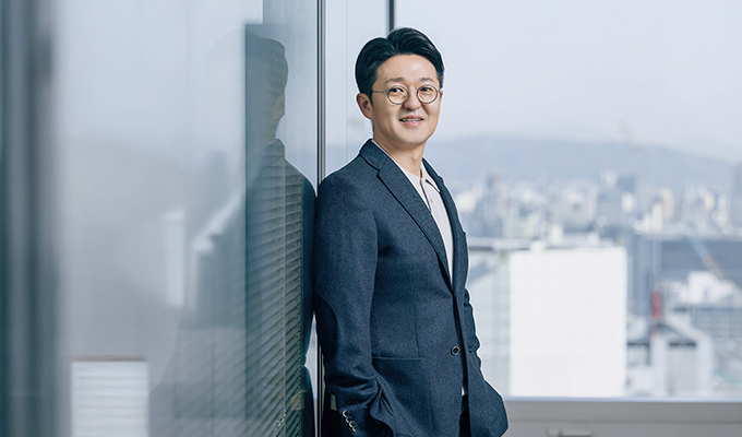
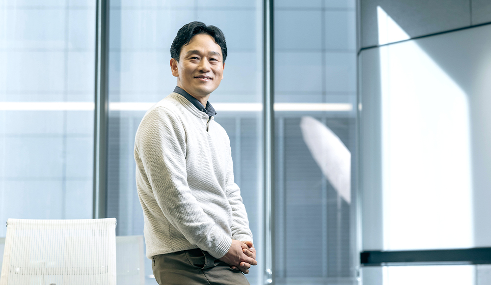
SK hynix newsroom met with Vice President Kyoungchul Jang, the newly appointed Head of VG TD at R&D, to discuss the importance of DRAM device technology in the AI era and the future of SK hynix’s DRAM technology.
Maintaing DRAM Market Leadership Through Technical Excellence
Since joining the company in 2008, Jang has built his career in device development. His work on DRAM cell device technology has earned him four SKMS Practice Awards and the Hynix Grand Award and has strengthened the competitiveness of SK hynix’s DRAM technology.
Reflecting on his appointment, Jang described the role as the culmination of his lifelong focus on a single field.
“Being appointed as an executive recognizes the dedication I have poured into this industry over the years,” Jang said.
“When I first started my career in this industry, my goal was to become a well-rounded semiconductor professional. Now, I believe it is time to fully put that commitment into action by giving my utmost effort.”
Jang cited maintaining SK hynix’s top-tier DRAM competitiveness as his greatest achievement to date. He expressed strong ambition to lead the next generation of development based on this success.
“The performance of SK hynix DRAM cells has consistently ranked No. 1, and I take great pride in carrying forward the achievements of my predecessors,” he noted.
“Keeping our ‘No. 1 DNA’ is not only our current strength but also the momentum for our next stage. Building on this, I will prepare for a new leap forward in SK hynix’s DRAM technology.”
Defining the Next Generation’s Standard at a Turning Point in DRAM Architecture
Jang described the present as a critical inflection point where DRAM architecture itself is undergoing a fundamental transition. At the forefront of this shift is the Vertical Gate (VG)1 TD organization, which is tasked with developing a new cell architecture that transcends the limits of conventional structures.
1VG (Vertical Gate): A next-generation DRAM cell architecture technology that implements a vertical gate structure to reduce cell area while achieving high density, high speed, and low power characteristics simultaneously.
“As the AI era gains momentum, customer demands are converging on greater capacity, faster speeds, and lower energy use,” Jang said. “As performance improvements through scaling nears the limit, a transition in cell architecture has become inevitable for sustainable innovation.”
To address this, Jang explained that DRAM processes must scale below 10 nanometers to increase density, alongside the development of a new DRAM platform leveraging VG architecture and wafer bonding2 to achieve both low power and high-speed performance.
2Wafer bonding: A process that precisely bonds different wafers to form a vertically stacked structure. It is an essential technology for implementing complex integration structures such as high-performance AI semiconductors.
“Our R&D directions and technological choices today will define the future competitiveness of SK hynix,” Jang said. “The mission of VG TD is to translate these choices into tangible products, setting the standard for the next generation of DRAM.”
To bring next-generation DRAM technologies to reality, Jang has identified enhancing the completeness of the new platform and securing early mass-production competitiveness as key priorities for this year. To this end, he plans to focus on technological optimization to enhance the integrity and reliability of new technologies, ensuring stable performance even in high-volume manufacturing environments.
“Our primary goal this year is to produce manufacturable chips while reducing TAT3,” Jang said. “To achieve this, we will thoroughly assess risks in advance to minimize delays and streamline execution.”
3TAT (Turn Around Time): The time required for development and verification processes.
Building a High-Execution ‘One-Team Spirit’ Culture
Jang emphasized that in a rapidly changing AI landscape, preemptive verification and swift execution are critical to securing differentiated competitiveness. He believes that meticulous preparation, coupled with the organizational capability to deliver immediate results, is essential to staying ahead.
“In order for an R&D organization to innovate, it must pursue the SUPEX spirit of bold challenge while maintaining constant and careful review,” Jang said. “Internally, every member must act with accountability andexternally, we must foster a ‘one-team spirit’ culture without barriers to support seamless communication.”
He is determined to foster a team culture centered on strong execution and collective strength.
“A leader’s role is not to demand perfection from every individual, but to connect individual strengths and overcome the limitations through team capability,” he said. “I will strive to create an environment where members can demonstrate their capabilities in their roles while the organization moves in one direction under a one-team spirit.”
In closing, Jang emphasized on the power of collaboration.
“Everytime we were developing a new technology, we questioned whether it was possible. But by achieving what once seemed uncertain, I became to appreciate the power of people working together,” he said. “SK hynix’s 2D DRAM, built by our colleagues, is world-class — and I take immense pride in that. As we navigate this critical turning point in DRAM structural transition, I will put my utmost effort to demonstrate the power of SK hynix’s people in VG DRAM.”