“We showcased our 4D NAND technology that will become the standard for the next generation.”
SK hynix’s Head of NAND development, Jungdal Choi, shared his thoughts after attending the Flash Memory Summit 2022 (FMS 2022), where SK hynix clearly demonstrated its competitiveness in cutting-edge technology in both DRAM and NAND, which dovetail nicely to lay the foundation for its future.
Flexing its technological muscle at FMS 2022, SK hynix is set to become a leader in ICT technology development. The current 4D NAND technology is recognized as an industry standard, thanks to its developers’ dedication and ceaseless efforts. The company also plans to continue supporting technological innovation that will help set the next-generation standard of 4D NAND technology.
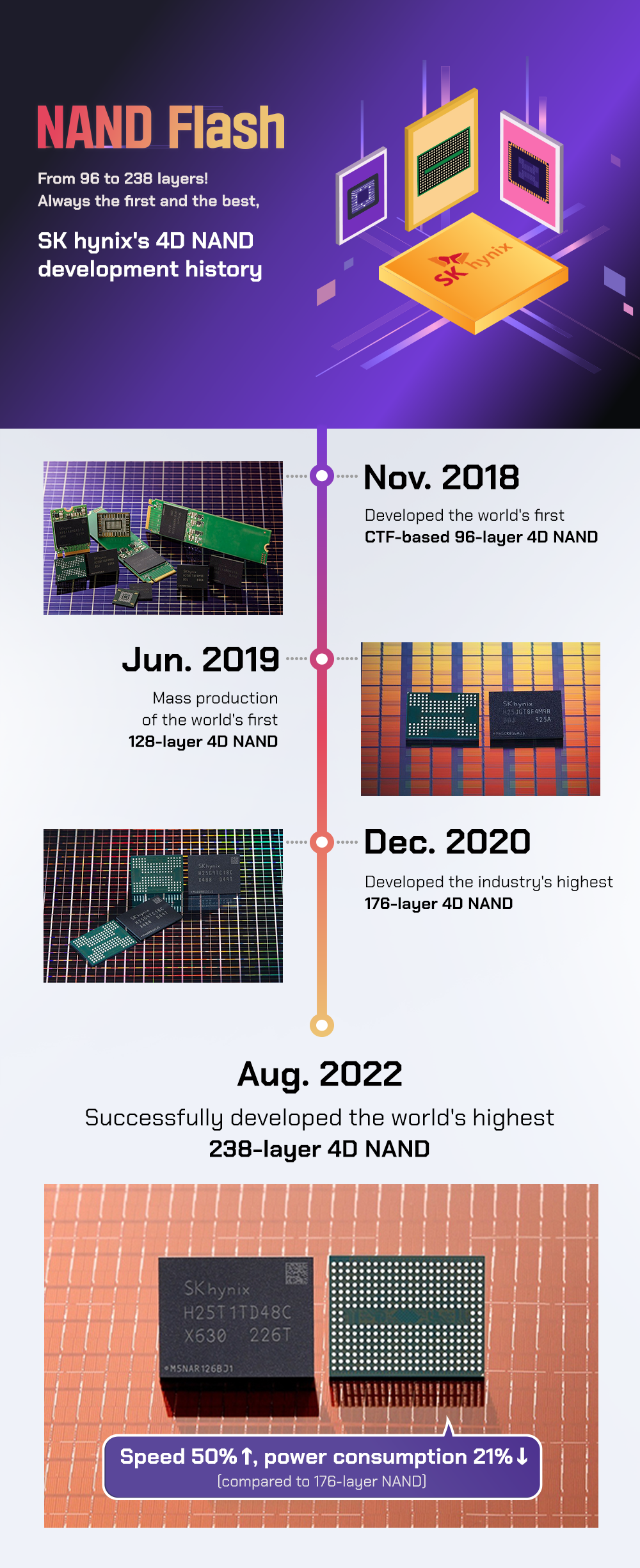
▲ Image 1. Jungdal Choi, Head of NAND Development, delivers his keynote speech at the Flash Memory Summit 2022.
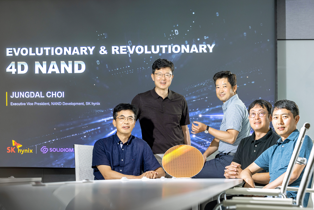
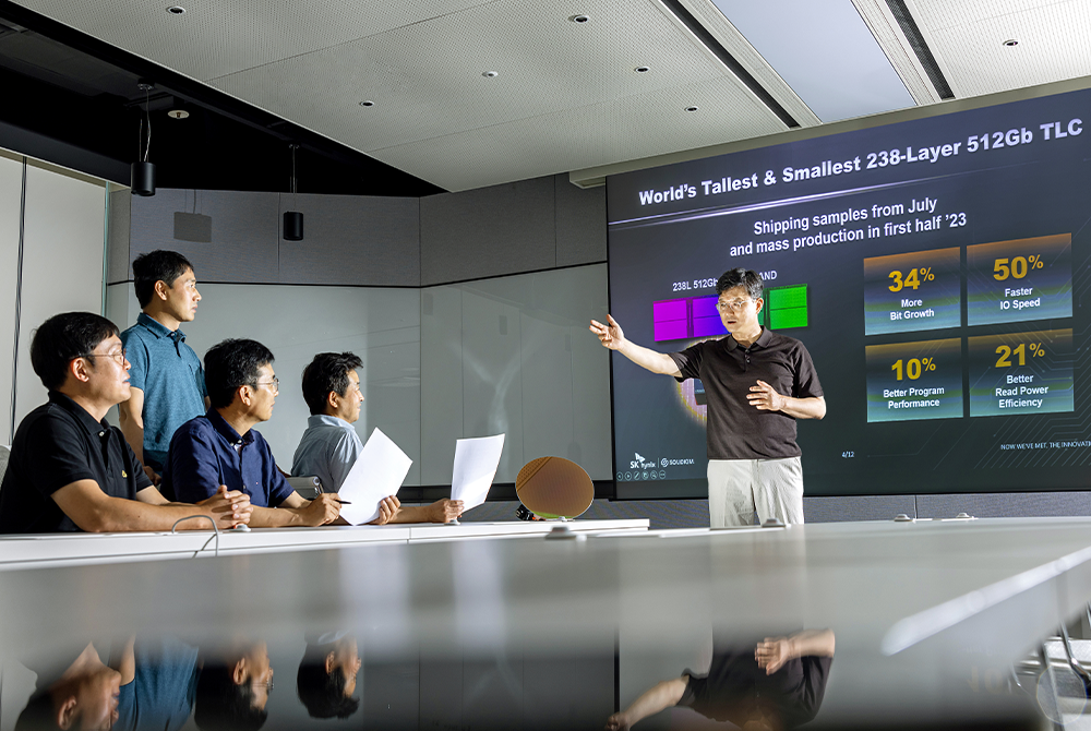
The Newsroom team hosted an FMS debriefing session, meeting with Jungdal Choi (Head of NAND Development), Jumsoo Kim (Head of S238 NAND), Jaesung Sim (Head of NAND QLC), Woopyo Jeong (Head of NAND Design), and Keumhwan Noh (Head of NAND PE C&R). Read on to hear snippets of the conversation, where the execs share their views on how they know SK hynix is poised to become the undisputed leader in NAND technology.
Showing the world 4D NAND’s core competitiveness
SK hynix was a key participant in FMS 2022, according to Jungdal Choi, Head of NAND development, where it introduced various products and new technologies including a 238-layer 512Gb (gigabit) TLC* 4D NAND (238-layer NAND). SK hynix’s 4D2.0 technology, which overcame the limitations of vertical stacking, was of particular interest.
*Triple Level Cell (TLC): NAND Flash products are categorized into Single Level Cell, Multi Level Cell, Triple Level Cell, Quadruple Level Cell and Penta Level Cell depending on the number of information (unit: bit) contained in a single cell. That a cell contains more information means more data can be stored within the same extent of area.
Choi, who spearheaded SK hynix’s presence at the event, explained the meaning of the participation and achievements as follows. “FMS 2022 raised SK hynix’s status through our differentiated NAND technology. It was a valuable opportunity to inform the world of SK hynix’s technological direction and of our 4D NAND core competitiveness,” Choi stated, giving an overview of the company’s goals and achievements at the event.
Q. What is the core competitiveness of 4D NAND?
Jungdal Choi NAND’s core competitiveness depends on securing the industry’s most stringent management in terms of scheduling, cost, quality, and performance, as well as developing competitive products with differentiated and unique technology. In 2018, we succeeded in commercializing our own industry-first, 96-layer 4D NAND, achieving the highest technological level in the industry. Additionally, based on our expertise accumulated from developing the 96-layer NAND, we developed the industry’s first 128-layer, 176-layer, and 238-layer NAND, gaining a technological advantage in the process.
The core technologies of 4D NAND that have led to these results are largely represented by three categories:
Sideway Source is a technology that horizontally connects the source, which is the electrons pathway. This technology lessens the dependence on the vertical structure of cell stacking and alignment issues between sources, and as a result, it is easy to secure yields.
All PUC (Peri Under Cell) is a technology that places the entire peripheral circuit (Peri.) under the cell. Thanks to this technology, chips size can be further reduced, and production efficiency is maximized.
Advanced CTF is a technology that stores electric charges in a CTF (Charge Trap Flash), which is an insulator, rather than a floating gate, which is a conductor. Compared to the floating gate storage method, cell area per unit can be reduced and read/write performance can be improved.
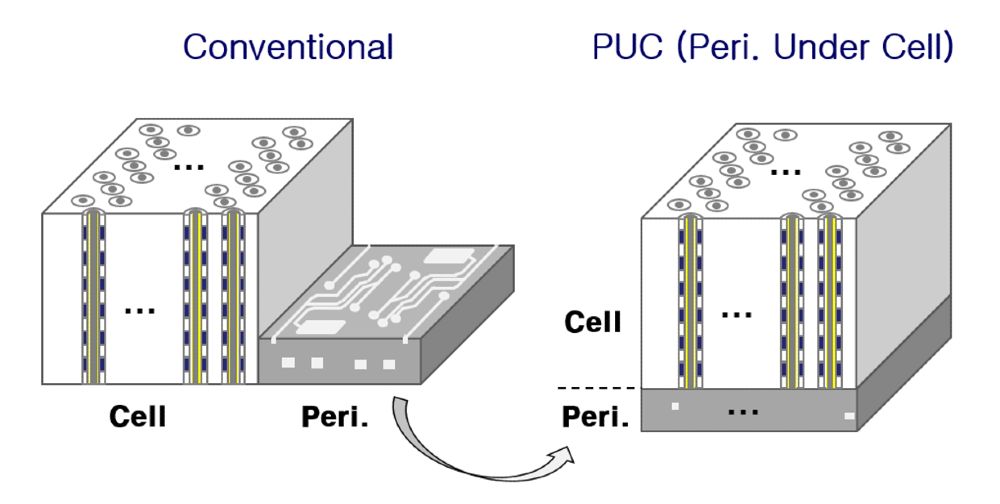
▲ Image 3. Peri. Under Cell (PUC): A technology that maximizes production efficiency by placing peripheral circuits under the cell array.
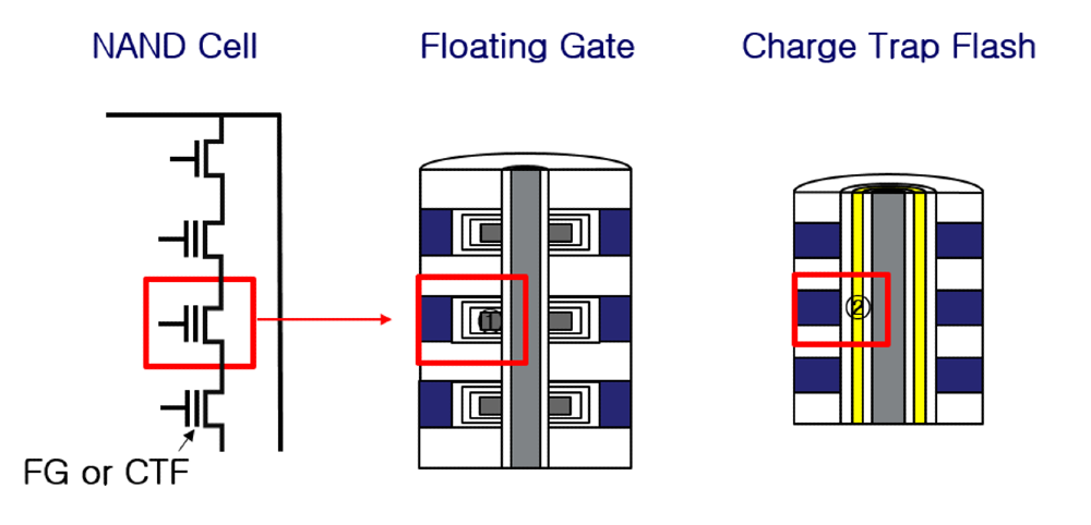
▲ Image 4. Charge Trap Flash (CTF): Unlike floating gate, which stores electric charges in conductors, CTF stores electric charges in insulators, which eliminates interference between cells, improving read and write performance while reducing cell area per unit compared to floating gate technology.
Q. Which products and technologies received most of the audience’s attention?
Jungdal Choi There was a lot of interest in the world’s highest and smallest 238-layer NAND flash. In addition to QLC, there were many questions about floating gate-based PLC and a software solution that can maximize the performance of CXL (Compute Express Link)*. People were very interested in the introduction of highest quality evaluation from customers and SSD products based on ultra-high-layered NAND. In addition, we are shaping the direction of technological innovation and serving as a leader in the NAND industry by defining next generation 4D NAND with 4D2.0 technology, which realizes both high capacity and performance while overcoming the limitations of cell stacking. I was able to feel firsthand that SK hynix’s technology and products are garnering interest.
*CXL: A next-generation interface for efficient utilization of high-performance computing systems. As a memory solution that can increase bandwidth and capacity cost-efficiently, SK hynix recently developed a 96GB CXL memory sample based on DDR5 DRAM.
Jungdal Choi These progressive and innovative technologies were achieved thanks to close collaboration with business partners and rooted in customer satisfaction. Most importantly, I believe that this success is based on the VWBE* initiative and the ambitious spirit among SK hynix employees, or “hy-gineers”, as we call them. The reason we were able to develop our proprietary technology and grow rapidly was thanks to our employees’ efforts and passion. We will not be satisfied resting on our laurels and will strive to continue to grow together.
*VWBE: Voluntary and Willing Brain Engagement. It is one of the employee values emphasized by SK Management System, or SKMS.
Surprise launch of 238-layer TLC 4D NAND, emphasis on technological superiority
As Choi pointed out earlier, the 238-layer NAND garnered a great deal of attention at the event. Jumsoo Kim, the head of S238 NAND who led the product development, said, “We garnered unprecedented attention as our chip size was reduced by more than 30% while applying advanced technologies such as the All PUC structure.”
Kim also emphasized that the product has technological advantages in cell writing speed (tPROG, the Programing Time), input/output speed (I/O speed), reading power efficiency, and bit growth.
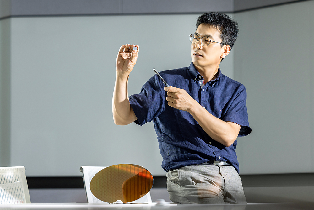
▲ Image 5. Jumsoo Kim, Head of S238 NAND, explains the 238-layer TLC 4D NAND’s technological superiority.
Q. Could you please explain the features of 238-layer NAND in a little more detail?
Jumsoo Kim When it comes to SSD performance, the most important factors are cell writing speed and I/O speed. Cell writing speed improved by 10% and this product also boasts speeds of 2.4 Gb per second, which is 50% faster than the previous generation, while reading power efficiency has also been improved by 20%. This is a product that meets market demand in a situation where customers are turning to low-power products.
Meanwhile, the products are also extraordinary in terms of bit growth: SK hynix can expect 34%-bit growth thanks to a dramatic reduction in the chip size.
QLC/PLC development is also on an upward trend… targets the future NAND market
SK hynix made a splash at FMS by unveiling 176-layer QLC NAND, 238-layer QLC NAND for mobile applications, and 192-layer QLC NAND adopting floating gate technology. In particular, the 176-layer 1Tb (terabit) QLC NAND doubled the I/O speed (1.6Gbps) compared to the 96-layer 1Tb QLC NAND and the read and write performance improved by 42% and 18%, respectively. “Our world record definitely stood out in the QLC area as well,” said Jaesung Sim, Head of NAND QLC, as he introduced the major products unveiled at the event.
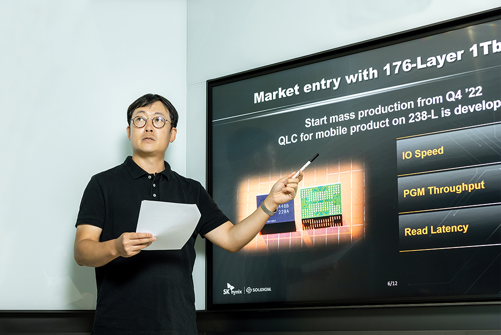
▲ Image 6. Jaesung Sim, Head of NAND QLC, explains the major products unveiled at FMS, including the 176-layer 1Tb QLC.
Q. What is the current development status of the 238-layer mobile QLC NAND and 192-layer QLC NAND?
Jaesung Sim We expect to do a full-fledged development for the mobile QLC. Accordingly, SK hynix is developing a 238-layer mobile QLC NAND. The 192-layer QLC for cSSD and eSSDs is also being developed by using floating gate technology with excellent multi-bit retention characteristics. Development of PLCs with a 25% increase in bit density per cell compared to QLC is also on the way as we speak.
Q. What efforts are you making to increase the number of stacks and bit density?
Jaesung Sim SK hynix pre-emptively developed 4D NAND technology and applied multi-row* technology, while rapidly changing the technological direction to multi-bit such as QLC and PLC. As a result, the company soon boasted the highest number of cell stacks and bit density in the industry. This was possible due to the quality maintenance process as well as design and testing technologies.
*Multi-row is a technology for continuously arranging multiple cell-stacked structures, similar to placing multiple apartment buildings next to each other in an apartment complex.
Introducing 4D2.0 technology while looking ahead to the next-generation technology standard
As one might assume from Sim’s explanation, SK hynix is continuously developing next-generation technologies that break through technological limits. This contributed to the introduction of the 4D2.0 technology.
4D1.0 reduces chip sizes by placing the NAND peripheral circuit (Peri.) under the cell area. With 4D1.0, chip sizes are reduced but the number of cell stacks must be increased. Although this has the advantage of being able to implement high density within a fixed area, the disadvantage is that the stacking technology could reach its limit. SK hynix solved this problem by horizontally increasing the cell density, a technological concept known as 4D2.0. According to Woopyo Jeong, Head of NAND design, this technology is expected to be the next-generation standard.

▲ Image 7. Woopyo Jeong, Head of NAND Design, explaining 4D2.0 that overcomes the stacking limit by increasing horizontal density.
Q. What is the core technology of 4D2.0?
Woopyo Jeong Multi-Site Cells (MSCs), which store data by dividing existing cells into two smaller cells via micro fabrication is the key, because we can expect to reduce the number of cell stacks while increasing cell density. For example, suppose that 6-bit data is stored in one cell. This can be implemented by combining the two signals 0 and 1 into 2*=64 different (voltage) states. However, it is very difficult to create 64 states in a limited voltage range.
However, if we use MSC technology, which combines two cells, we can implement a total of 64 (8×8) states by creating 3 bits per cell, that is, 2*=8. As a result, the 3-bit MSC secures the same capacity as a 6-bit cell, which is difficult to implement using a single cell.
Q. What will the future of the NAND market that 4D2.0 will create look like?
Woopyo Jeong If vertical stacking and size reduction are repeated, cell quality inevitably deteriorates. Therefore, in the future, it will be difficult to increase data capacity using only stacking technologies. However, 4D2.0, which utilizes MSCs as the core to horizontally increase density, can overcome this limitation. This is expected to become an industry standard in the future.
As technology becomes more sophisticated, quality is our top priority
As NAND technology advances, it will be difficult to secure the best quality. SK hynix also faced numerous difficulties during the development process and had no choice but to work harder at improving quality. Accordingly, Keumhwan Noh, Head of NAND PE C&R, emphasized quality as a top priority, saying, “The excellent quality of SK hynix will continue in the future.”
In a recent quality evaluation survey of major mobile and SSD companies, SK hynix’s 128-layer and 176-layer NAND products ranked first. Noh argued that the stabilization of the 4D NAND development platform and mass production was the main reason, along with the significantly reduced number of defects. SK hynix is currently developing new products based on stabilized processes and is planning to introduce various quality improvement technologies and solutions.
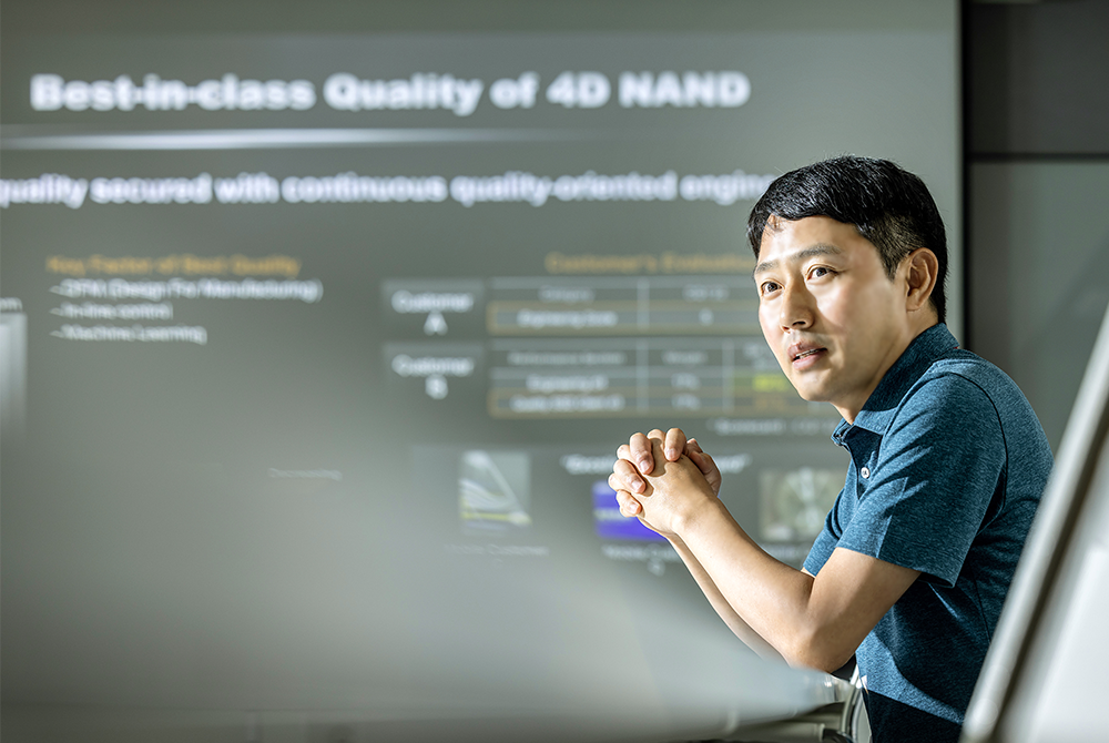
▲ Image 8. Keumhwan Noh, Head of NAND PE C&R, reveals challenges related to NAND quality improvement.
Q. What are the biggest issues related to quality and the challenges ahead?
Keumhwan Noh As the number of cell stacks continues to increase, the gap between cells will become narrower. Therefore, it is highly likely that defects in the cell region will increase. To respond to these issues, SK hynix is seeking a wide array of measures such as strengthening NAND Design for Manufacturing (DFM)* initiative, reinforcing inline management, source quality advancement using AI machine learning, and controlling defects by utilizing solution algorithms.
*DFM (Design for Manufacturing): Design in consideration of the manufacturing environment, which makes a reliable product or a design for productivity.
SK hynix plans to upgrade its products in line with technological trends, mass-produce 238-layer NAND in the first half of next year, and consecutively release mobile-oriented products, cSSDs and eSSDs. In order to respond to high-capacity demand, the company is preparing 238-layer 1Tb QLC products, strengthening multi-bit storage capacity from QLC to PLC, and preparing the next-generation technology of 4D2.0.
After the session, Jungdal Choi said, “Looking back at the ICT industry over the past 10 plus years, only companies with their own unique technology were able to secure their status as top global technology companies. We will maintain our competitiveness through successful ramp-ups (yield improvement) of 4D1.0 and innovation with our proprietary 4D2.0 NAND technology.”