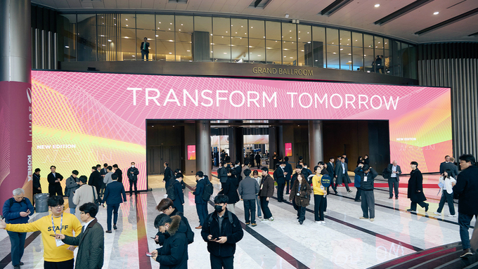
SK hynix is showcasing its R&D capabilities and technology innovation roadmap at SEMICON Korea 2026, Feb. 11-13, underscoring the company’s leadership in the global memory market.


Hosted by Semiconductor Equipment and Materials International (SEMI), SEMICON Korea is the country’s leading exhibition for the semiconductor industry, convening a range of global companies under one roof. This year’s event is the largest to date, with exhibition space expanded beyond the main venue. A total of 550 companies are operating 2,411 booths, showcasing advanced semiconductor technologies and solutions, and numerous semiconductor industry professionals are attending the exhibition, sharing their insights on the latest global trends.
Industry executives and technology leaders from major global semiconductor companies are delivering keynote speeches, introducing a range of technological innovations and process optimization approaches required in the AI era while bringing attention to key topics on the industry’s mid- to long-term direction, supply chain development, and collaboration strategies.
Alongside the exhibition, the SEMI Technology Symposium (STS) is gathering engineers to share the newest technology trends across process areas and to explore solutions to key challenges currently in research and development. In addition, tutorial sessions, which provide early-career engineers and students with fundamental process knowledge and cutting-edge insights, are also being successfully held concurrently with SEMICON Korea.
Rethinking R&D Through AI-Driven Innovation and New Collaboration Models
SK hynix delivered a keynote address, presented STS sessions across six themes, and offered tutorial sessions in three subjects, reaffirming its position as a technology leader in the memory semiconductor field.


Lee Sunghoon, Senior Vice President of R&D Process at SK hynix, delivered a keynote address titled “The Inflection Point Has Arrived: Driving Innovation Towards the Future of Memory Technology,” in which he introduced the company’s ongoing AI-powered innovations in research and development.
As semiconductor processes become more complex, the technology applied to those processes are likewise becoming increasingly sophisticated. DRAM has already entered sub-10nm nodes, while NAND has transitioned from 2D to 3D architectures — in other words, technical difficulty is rising sharply, exceeding the previous rate of increase. As a result, both the time and amount of resources needed to secure next-generation technologies are also rising.
“Despite these challenges, SK hynix has secured key technologies in a timely manner by systematically forecasting technological difficulty levels and collaborating with partners,” Lee explained. “By moving beyond the existing product-by-product development method and introducing a platform concept that can be commonly applied across multiple generations, we have streamlined the development process and effectively suppressed increases in the development cadence.”1
1Development cadence: the interval between the completion of one technology and the next
However, the limits of DRAM scaling are becoming apparent, while NAND is moving toward ultra-high stacking levels. As a result, another technological inflection point is expected to emerge beyond 2027. “In order to effectively respond to the upcoming inflection point, we require structural advances to overcome technical challenges and material innovation to respond to growing technological complexity,” Lee explained. “We must actively pursue the convergence of technologies while exploring new AI-based collaboration models.”
In particular, Lee highlighted the potential of AI technologies to significantly reduce the time and effort required to explore new structures or evaluate whether new materials are suitable for a process. As one example of AI utilization, he presented a case study that optimized process simulations developed in collaboration with NVIDIA.
“AI models enable a far broader range of materials to be evaluated within a shorter period compared with conventional methods, while also making it easier to identify optimal process conditions with fewer experiments,” Lee remarked. He added, “The industry must move beyond traditional ‘man-month’-based R&D, which relies on increasing manpower, toward AI-based R&D, which amplifies time efficiency.”
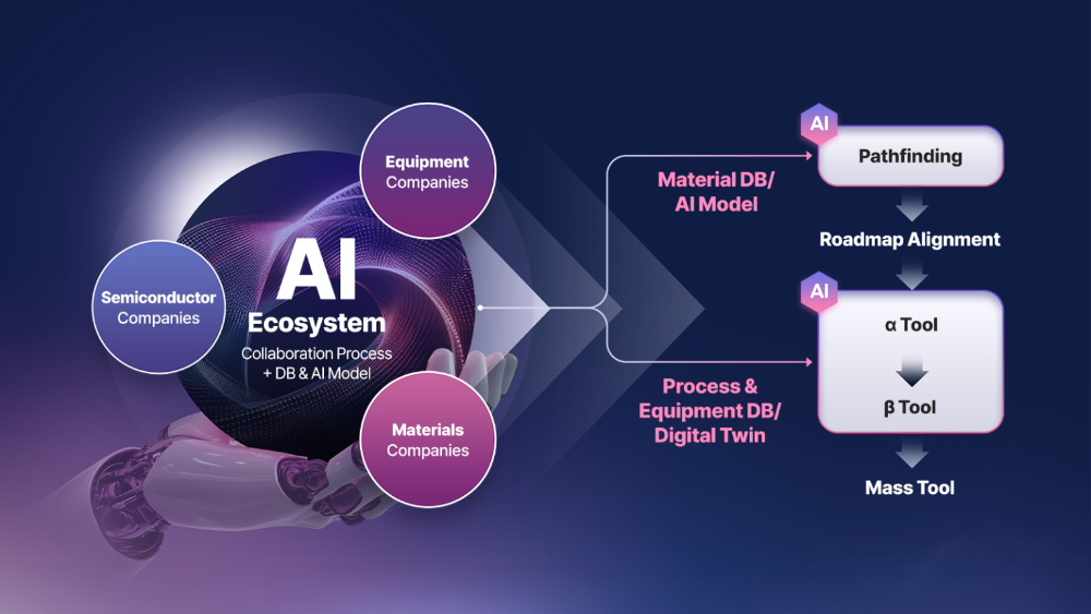
Lee highlighted data management and AI models as key factors in advancing AI-based R&D innovation. “As the industry approaches another technological inflection point, AI-based R&D is not a challenge unique to SK hynix but a shared task that the entire semiconductor industry must solve together,” he stated. “At this juncture, the industry needs to consider how to address long-standing challenges related to data sharing among collaboration partners — an area traditionally constrained by IP protection — and how to build collaborative systems that leverage common AI models,” he continued, raising new points for industry-wide discussion.
“If we can build an AI ecosystem that can be shared with partners and effectively integrate it with existing collaboration frameworks, we will be able to maintain the current development cadence even in the near future, when technological complexity is expected to increase dramatically,” Lee shared, while reaffirming the company’s intention to maintain its current edge amid future technology competition.
SK hynix Shares Advanced Process Technologies and Manufacturing Expertise at STS Sessions
At the STS sessions held Feb. 11-12, SK hynix employees presented in six technology sessions, sharing the company’s latest process technologies and manufacturing expertise.


SK hynix employees presenting during STS sessions
Kim Hongik of DRAM Track Photo presented approaches to effectively utilize a high-numerical aperture extreme ultraviolet (high-NA EUV)2 lithography system in the Advanced Lithography session, while Oh Jinho of the Future Technology Research Institute discussed the technical challenges associated with ultra-high NAND stacking and the efforts to address such challenges in the Advanced Materials & Process Technology session.
2High-numerical aperture extreme ultraviolet (high-NA EUV) lithography: A next-generation lithography technology that adopts a higher numerical aperture (NA) than conventional EUV, significantly enhancing the resolution used in equipment to pattern circuit features onto semiconductor wafers
Noh Yoohyun of NAND TD shared device and process technologies being secured for next-generation NAND implementation during the Device Technology session, while Park Sangwook of Plug Etch reviewed the latest trends in high aspect ratio contact (HARC)3 technologies in the Plasma Science and Etching Technology session.
3High aspect ratio contact (HARC): an etching technology used to create fine contact holes with a high aspect ratio
In addition, Lee Hyeokjung of DRAM C&C addressed optimal overlay (O/L) control conditions for effective chemical mechanical polishing (CMP)4 processes in the CMP & Cleaning Technology session. Finally, Sung Kijun of PKG Innovation provided a detailed explanation of vertical wire fan-out (VFO)5 technologies for on-device AI in the Advanced Packaging session.
4Chemical mechanical polishing (CMP): a process that planarizes thin films on wafers by polishing surface irregularities using chemical and mechanical methods
5Vertical wire fan-out (VFO): a technology that vertically connects wire bonding to minimize space and reduce power consumption
“Through SEMICON Korea, we were able to demonstrate SK hynix’s outstanding technological capabilities and highlight the various efforts underway across the organization to drive innovation,” a company representative stated. “As a full-stack AI memory creator, we will continue to strengthen our technology leadership to meet customer needs and sustain our competitive edge in the AI memory market.”