As the AI era accelerates, semiconductor manufacturing processes are now requiring an unprecedented level of precision and quality. Beyond simply scaling down circuit size, the ability to mass-produce increasingly complex designs with high reproducibility and stability has become critical. In an environment where demand for both performance and integration density is rising, the precise translation of design intent onto wafers has become a key factor in semiconductor competitiveness.
Among many technologies driving SK hynix’s AI-era breakthroughs, photolithography1 has played a pivotal role, quietly enabling an extreme level of precision.
Each finely designed pattern formed through photolithography technology directly impacts product performance, yield, and cost competitiveness, further underscoring the importance of the Photo Technology department.
1Photolithography: A process that transfers circuit designs onto a wafer using light, directly determining semiconductor performance and integration density
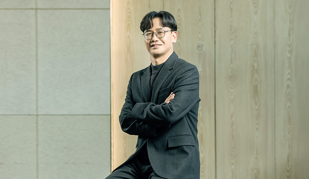
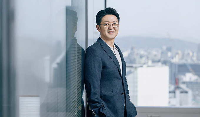
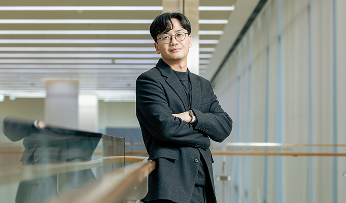
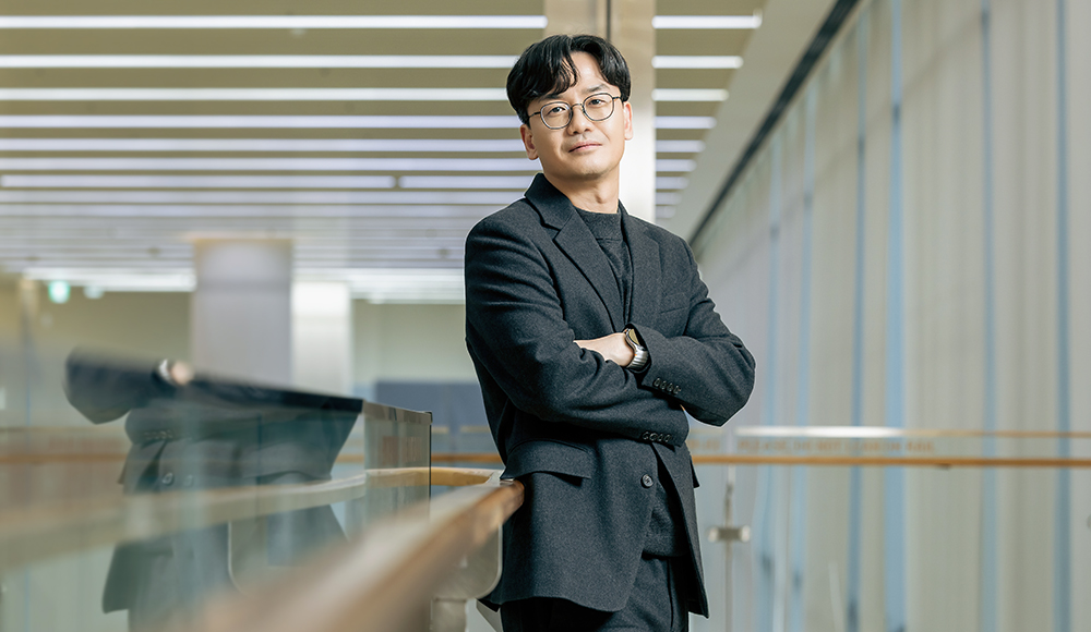
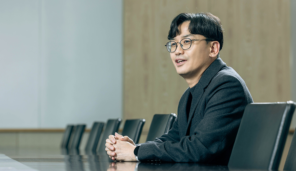
With the new appointment of Vice President Hyunsok Kim, head of the Photo Technology department, SK hynix is preparing for the next wave of technological innovation. The SK hynix Newsroom met with Kim to discuss his vision for the company as well as his strategic roadmap for the Photo Technology department in the AI era.
Profound Responsibility at Critical Moment
Kim is a technology expert who has pushed the boundaries of technology in the photolithography sector since 2004. A true engineer at heart, Kim used to be driven by the sense of accomplishment he felt when achieving the seemingly impossible, such as inscribing microscopic patterns on wafers. Now as head of the Photo Technology department, he says he has a different motivation, a sense of responsibility.
“I’m honored to take on such an important role at this pivotal juncture in the AI transformation, but I also feel a profound sense of responsibility,” Kim shared. “Moving beyond my past role as an engineer, I now stand at a new starting point where I must consider the broader direction and mission of the entire organization. As a leader who sees not just the trees but the entire forest, I pledge to guide the Photo Technology department forward.”
Kim regards his appointment as a reflection of SK hynix’s expectations and a call to action for the Photo Technology department. As global competition for technological dominance intensifies, he emphasized the growing importance of the department, expressing confidence in steering the department through this critical period.
“I believe photolithography is the core technology that will solve the increasingly complex challenge of semiconductor scaling,” Kim emphasized. “Drawing on the expertise I’ve accumulated in the field, I’m committed to building a Photo Technology department that fully meets the company’s expectations.”
Photolithography, the ‘Master Key’ To Becoming a Full Stack AI Memory Creator
In 2025, SK hynix further solidified its position as the leader of the AI memory market. Amid that momentum, Kim cited the stabilization of the extreme ultraviolet (EUV)2 process as the most meaningful achievement of the Photo Technology department.
2Extreme ultraviolet (EUV): A lithography technology, using short wavelengths of light (extreme ultraviolet), is used to etch circuit patterns onto wafers.
“Recently, the Photo Technology department made a significant improvement in EUV process stability, enabling the successful development of 1c3 DRAM and contributing to the timely development of High-Bandwidth Memory (HBM),” Kim explained. “I consider this our greatest achievement. Implementing ultra-fine patterns involves numerous technical challenges, but our department overcame them one by one, elevating our capabilities to the next level.”
31c: The sixth generation of the 10nm-class DRAM process technology, which was developed in the order of 1x-1y-1z-1a-1b-1c. In August 2024, SK hynix unveiled the world’s first 1c DRAM technology.
“As scaling approaches its limits, the ability to manage EUV technology efficiently and reliably will determine both product quality and cost competitiveness,” Kim emphasized. The process stability secured by the Photo Technology department serves as a powerful platform for accelerating development across the next-generation roadmap. “This achievement will become a technological asset supporting both ‘time to market’ and qualitative growth,” he added, underscoring his commitment to strengthening mid-to-long-term competitiveness.
In particular, as SK hynix advances its vision of becoming a full-stack AI memory creator in 2026, Kim defined the role of the Photo Technology department as the “master key” to realizing future memory technologies.
“Our vision of becoming a full-stack AI memory creator means delivering customer-tailored value at every stage — from design to process and packaging — in response to increasingly diverse demands in the AI era,” Kim said. “As the driving force behind both product performance and mass-production competitiveness, the Photo Technology department serves as the master key to unlocking future memory competitiveness. In response to the AI era, we plan to establish a smart, data-driven photolithography process to secure stable yield and quality across diverse custom product environments.”

First to lead. Last to leave.
Kim has a clear vision of leadership: to lead from the front while standing alongside his team until the very end. To do so, he believes that a leader must first become a rigorous expert with deep technical expertise.
“In my view, a true leader sets the direction from the front and takes responsibility alongside the team until the very end. To make this possible, technical expertise and a collaborative culture that breaks down organizational boundaries must go hand in hand,” Kim shared. “Technical excellence is the foundation of an organization’s competitiveness and confidence, while a ‘one-team spirit’ is the force that turns that competitiveness into tangible results. I believe that when the Photo Technology department becomes a central hub of collaboration combining these two pillars, we can transform our vision of becoming a full-stack AI memory creator into reality.”
At the end of the interview, he shared a New Year’s message with SK hynix employees, emphasizing the importance of embracing challenges.
“We are now at the forefront of a rapidly changing era for the semiconductor history. While we’re experiencing a period of unprecedented growth, there are also concerns about technological limits,” Kim stated. “However, I believe this is precisely the moment for us to take on new challenges and achieve the next stage of growth. Whatever technical challenges arise, there is nothing we can’t accomplish if we work together as one team. I hope we can build an SK hynix where every employee embraces the spirit of challenge, shares in the rewards of our collective efforts, and genuinely encourages one another along the way.”