AI doesn’t wait. The foundations of every industry are already cracking. This isn’t a story about one sector. Manufacturing. Finance. Healthcare. Data centers. The entire industrial order is being rebuilt around AI — and it’s happening now. Knowing about AI is no longer a competitive advantage. You need to see through it. That’s why our Newsroom is putting AI — and the semiconductors that power it — under the microscope.
In the first installment of the [Tech Note] series, we sit down with SOD, CEO of Heisenberg — a Korean science, technology, and IT creator and one of the leading voices in specialist tech media — to explore what the AI revolution really means for the road ahead.
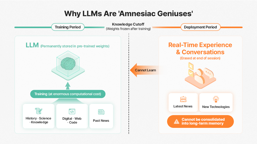
The Amnesiac Genius at the Heart of Today’s AI
Imagine you have an extraordinarily talented assistant — brilliant, capable of completing any task you assign with flawless precision. There’s just one problem: every morning, they arrive at work with no memory of the day before. Your name, your company, the project you briefed them on yesterday — gone. You have to start from scratch every single time.
Frustrating? Absolutely. But according to Kim Juchan, a semiconductor device researcher at KAIST (Korea Advanced Institute of Science and Technology), this scenario isn’t hypothetical. It’s an accurate description of the AI systems we rely on today.
‘The Amnesiac Genius’
ChatGPT, Gemini, Claude — the large language models (LLMs) we call “intelligent” are, in a clinical sense, suffering from ‘Anterograde Amnesia’. They can recall everything they were trained on — a vast archive of human knowledge compiled at enormous cost by the world’s biggest tech companies — but they cannot form new long-term memories after that training ends.
To compensate, those same tech companies are burning through vast quantities of GPUs and HBM, forcing models to re-read entire conversation histories with every new query. It’s the computational equivalent of photocopying an entire library every time you want to borrow a single book.
Continual Learning and the Titans Architecture: Reshaping the AI Stack
Starting in 2026, the competitive dynamics of AI are expected to shift fundamentally. Kim anticipates that the commercial rollout of Google’s Continual Learning1 framework and the Titans Architecture2 will trigger the collapse of Static Inference3, as we know it today. Rather than training once at massive scale and then freezing model weights for inference, the boundary between training and inference will dissolve — inference itself performing fine-grained weight updating to enable continuous post-deployment learning.
1Continual Learning: A multi-speed, multi-layer update paradigm in which a model incrementally learns from new data without catastrophic forgetting of prior knowledge.
2Titans Architecture: A next-generation AI model architecture designed by Google that combines Attention (for short-context processing) with Neural Memory (for long-term information storage) to handle extended context windows efficiently.
3Static Inference: The conventional inference mode in which pre-trained model weights remain frozen; model parameters are not updated during the inference process.
The term “Static Inference” describes the AI paradigm that has defined the field until now. Adapting a trained model to new domains forces engineers to invest significant time and compute budget in resource-intensive fine-tuning4. The human brain, by contrast, operates very differently. The instant you touch a scorching kettle, your brain encodes the danger in long-term memory within milliseconds, immediately recalibrating synaptic connection strengths — all without rewriting the brain’s fundamental architecture.
4Fine-tuning: The process of re-training a pre-trained foundation model on task-specific or domain-specific datasets to optimize performance for targeted applications.
The Titans Architecture approaches memory not merely as passive data storage but as active, human brain-like memory management. It selectively updates memory only when the model detects a ‘Surprise’ input — unexpected, novel information — enabling Test-Time Training (TTT): the model’s inference process itself becomes a continuous learning loop, enabling AI that grows without ever stopping.
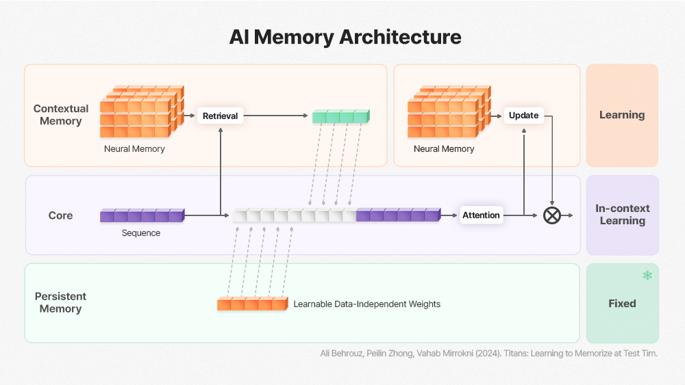
These architectural changes carry profound implications for hardware. Existing memory semiconductors — DRAM and HBM — were fundamentally designed around a Read-Heavy access pattern: HBM reads data, feeds it to the GPU for computation, then writes results back. With Continual Learning integrated into the inference pipeline, this model breaks down.
As AI models continuously update weights during inference, the memory subsystem must now handle frequent Read-Modify-Write (RMW) operations. Simply scaling memory bandwidth cannot absorb this weight-update traffic surge.
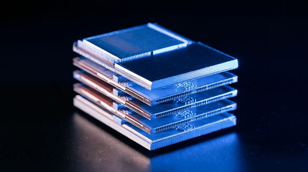
The short-term memory module (Core) of the Titans Architecture, analogous to human working memory, changes state rapidly — demanding capabilities beyond raw bandwidth. Effectively managing this module will require memory that can perform in-situ computation, pointing toward next-generation HBM (post-HBM4) with compute logic embedded in the base die, or PIM (Processing-In-Memory)5 technology. When data is processed inside the memory itself rather than shuttling back and forth across the memory bus to the GPU, real-time learning efficiency improves dramatically.
5PIM (Processing-In-Memory): A next-generation memory architecture that integrates processing logic directly into the memory die, eliminating the traditional von Neumann bottleneck between memory and processor, dramatically improving bandwidth efficiency and energy consumption
The explosion in data volume that accompanies Continual Learning also creates a new economic challenge. HBM carries a significant cost premium, making it economically infeasible to store all data on-stack. This has directed industry attention toward HBF (High Bandwidth Flash)6, a new memory tier leveraging the CXL (Compute eXpress Link)7 interface to bridge the performance gap between HBM and SSD.
6HBF (High Bandwidth Flash): An emerging memory tier positioned between HBM and SSD, combining HBM-class bandwidth characteristics with the high-density capacity of NAND flash-based storage, designed to improve scalability and power efficiency across AI infrastructure.
7CXL (Compute eXpress Link): A high-speed interconnect interface standard that enables memory and processor resources within a system to be efficiently pooled and expanded beyond single-device limitations.
SK hynix — which holds a dominant competitive position in HBM — has already initiated proactive R&D to secure next-generation high-bandwidth storage technologies including HBF, signaling that the company is not content to rest on HBM leadership alone [Related Article]. The evolution of AI algorithms is quite literally redrawing the hardware roadmap.
From ‘Faster Memory’ to ‘Predictable Memory’
The AI systems of the future are unlikely to operate with a single, monolithic memory architecture. Taekyoon Park, a researcher currently at Siemens with prior experience at leading Korean semiconductor firms, reflects on the past decade of memory technology development as a relatively linear scaling trajectory.
Historically, the memory market evolved in generational lock-steps — DDR3 → DDR4, HBM2 → HBM3 — with each new generation displacing the previous one through superior speed and density. But going forward, memory architecture is likely to fragment significantly, with specialized tiers serving distinct workloads rather than a single dominant standard.
Meanwhile, the momentum of AI model scaling is visibly decelerating — a consequence not of fundamental technical limits, but of compounding real-world constraints: training cost, power consumption, and time-to-deployment. The diminishing marginal returns of simply scaling model parameters are becoming apparent, and the compute and capital required to train and sustain frontier LLMs have reached a threshold accessible only to select few hyperscalers.
Park points out that “when designing or operating AI systems in the field, it is quite common to find that a system with theoretically sufficient memory specifications still falls short of expected performance in a real-world production environment.” He further notes a growing number of cases where even systems equipped with high-performance memory such as HBM experience repeated latency spikes and performance instability under specific workloads.
Yet in many cases, this phenomenon is not attributable to a raw bandwidth shortfall in HBM itself. Rather, it originates from the mismatch between average memory throughput and the deterministic response characteristics demanded by live service environments. While mean performance may be well within spec, a single latency outlier at a critical moment can disproportionately degrade overall system performance — and that, Park emphasizes, is where the real problem lies.
Against this backdrop, semiconductor industry players are converging on a new consensus: latency-centric8 memory will increasingly decide competitive outcomes in the industry. As real-world deployments continue to demonstrate that Tail Latency9 — not average bandwidth — is the variable that ultimately governs system reliability, memory architects and chip designers are shifting their priorities accordingly.
8Latency-centric: A system design philosophy and market segment that prioritizes individual response time (latency) as the core performance metric over average throughput or aggregate bandwidth.
9Tail Latency: The worst-case latency experienced by a small fraction of requests — typically the 99th or 99.9th percentile. In large-scale distributed systems, tail latency has outsized impact on end-to-end service stability and perceived performance.

Consider a humanoid robot that executes dozens of balance-correction decisions per second. Even if 99.9% of those decisions are processed within the required time window, a single memory-bottleneck-induced latency spike can cause a catastrophic fall. Average performance can be excellent; a single outlier event can compromise the entire system.
As NVIDIA CEO Jensen Huang emphasized at both CES 2025 and CES 2026, the AI industry is on a clear trajectory toward the era of Physical AI10. In this environment, memory predictability — the ability to deliver consistent, deterministic response characteristics — stands to become a more decisive competitive differentiator than peak throughput.
As AI deployment scenarios continue to diversify, the hardware requirements they impose on the underlying memory architecture are pulling the industry in fundamentally different directions. Frontier model training clusters, robotic AI systems running continuous factory surveillance, and agentic AI platforms serving tens of millions of concurrent users each demand a fundamentally different set of physical performance requirements — a reality that no single, monolithic memory architecture can adequately address.
10Physical AI: AI deployed in physical systems — including robots, autonomous vehicles, and industrial automation equipment — that must interact with and operate within the physical world in real time.
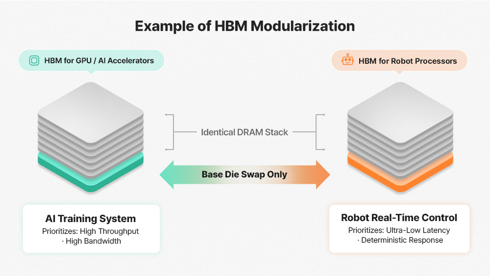
This divergence in workload requirements raises a fundamental design question for the memory industry. If every customer demands a distinct performance profile, AI memory providers such as SK hynix may need to engineer dozens of differentiated HBM variants — each tuned for a specific use case. In practice, however, this approach runs into hard limits on both manufacturing efficiency and yield optimization.
Park suggests that HBM will increasingly evolve toward a custom HBM (cHBM) architecture — where hardware specifications are tailored to the demands of each specific workload. Rather than redesigning the full HBM stack for each customer, the Base Die — the controller and PHY logic layer at the bottom of the HBM stack — becomes a configurable variable.
Training clusters that prioritize sustained memory bandwidth would be paired with a bandwidth-optimized Base Die; robotic and real-time control systems requiring deterministic response would leverage a latency-optimized Base Die instead. The result is a composable architecture — one in which standardized components can be reconfigured like building blocks to meet the full spectrum of AI workload demands.
6G and AI-RAN: The Hidden Battleground
The architectural transformation described above extends far beyond the memory subsystem. Autonomous vehicles, Physical AI, and UAM (Urban Air Mobility) systems all depend not only on high-performance GPU/memory compute but on robust, deterministic communication infrastructure that can support them at scale.
Minwoo Kim, an AI communications researcher at POSTECH (Pohang University of Science and Technology), argues that the defining innovation of 6G is not simply higher speed — it is the delegation of network control to AI. Where legacy wireless networks operated under human-defined protocols, 6G will introduce AI-RAN (AI Radio Access Network)11, enabling base stations to analyze and optimize spectrum allocation, data routing, and network state in real time.
11AI-RAN: An architecture that embeds AI within the Radio Access Network (RAN) layer of cellular infrastructure, enabling real-time autonomous optimization of frequency resource allocation, data path routing, and network management.

These shifts are fundamentally redefining the nature of telecommunications infrastructure. NVIDIA’s move into the AI-RAN Alliance — extending its footprint well beyond compute and into the telecom domain — is a clear signal of where the industry is heading. With approximately 12 million base stations deployed globally, the introduction of AI accelerators into cellular infrastructure opens an entirely new AI infrastructure market at scale.
Practical challenges, however, are already emerging. Telcos want to dual-purpose their base station AI accelerators — running MEC (Multi-access Edge Computing) workloads and generative AI inference during off-peak hours rather than leaving expensive hardware idle. But when these service-layer tasks compete for the same compute resources as live network traffic, latency-sensitive systems such as autonomous vehicles face the risk of real-time communication delays they cannot afford.
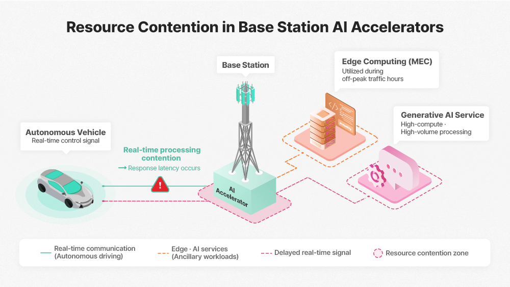
In a 6G environment, this makes memory isolation and virtualization — the ability to enforce a hard separation between telecom-dedicated and service-layer resources within a single physical node — a critical technical requirement. Kim warns that this is a challenge commodity memory architectures are fundamentally ill-equipped to handle, and identifies 2026 as a pivotal year in which industry players will set the direction of the relevant standards.
Memory Semiconductors: Driving the AI Era
Underlying every challenge discussed above is a single, unifying bottleneck: Data Movement. In today’s conventional computing architecture, the repeated cycle of fetching data from memory, transferring it to the compute unit, and writing results back extracts a steep cost — in energy consumption and processing latency alike.
The author first encountered this problem up close in 2022, when an SK hynix internal broadcast offered an early look at PIM technology. That perspective sharpened further at the SK hynix booth at CES 2025, where a direct encounter with AiM (Accelerator-in-Memory)12 technology made the case for on-chip compute impossible to ignore. When computation happens inside the memory die itself — eliminating the round-trip to the GPU — performance and energy efficiency improve in tandem. More fundamentally, this is the physical infrastructure that makes Continual Learning viable: not just a software architecture, but a hardware reality that Kim’s vision depends on.
12AiM (Accelerator-in-Memory): Next-generation solution incorporating processing capabilities within memory
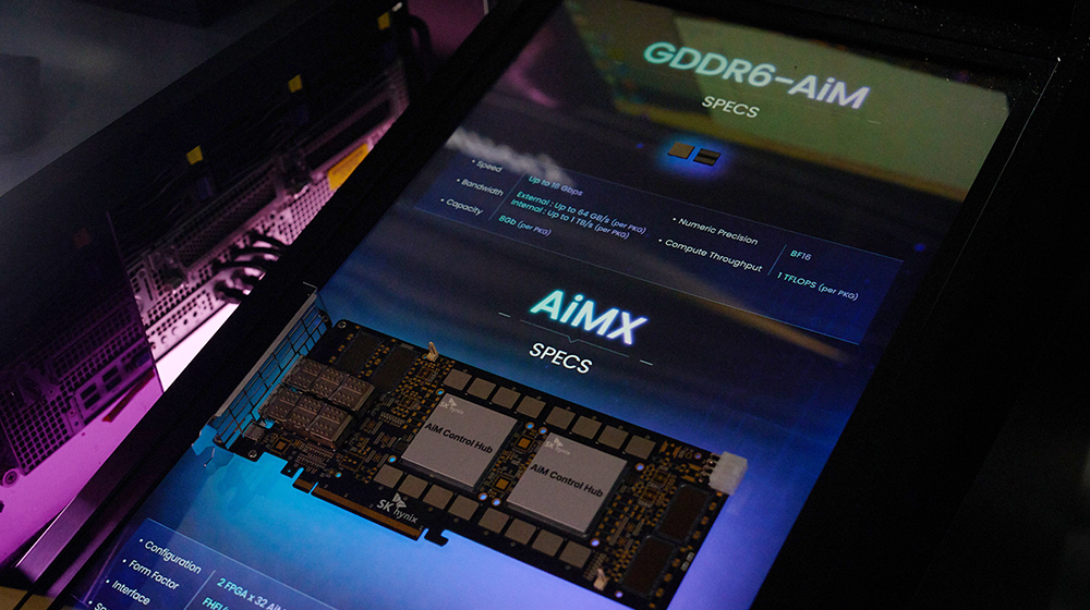
In a Continual Learning environment, frequent compute operations and on-the-fly weight updates generate a sustained stream of Read-Modify-Write (RMW) traffic. A PIM-based memory architecture such as GDDR6-AiM can substantially reduce the bottleneck between GPU and memory by absorbing and processing this traffic directly within the memory die. When memory updates model weights in-situ — without routing data to and from the GPU — the architecture eliminates round-trip latency, making a genuinely real-time learning pipeline possible. Ultimately, fully realizing the AI era demands a fundamental architectural evolution well beyond what conventional memory design can offer.
Against this backdrop, the rationale behind SK hynix’s planned approximately $400 billion (₩600 trillion) investment in the Yongin Semiconductor Cluster become clear. This is not simply a capital expansion — it is a proactive strategic move driven by a structural shift in the AI industry, and a clear signal of where the company believes competition will be decided.
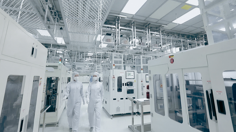
The gap between a cleanroom built in 2019 and one built in 2026 illustrates just how dramatically the technical bar has been raised. Process scaling and the growing density of manufacturing equipment have expanded the required cleanroom footprint — driving up both construction costs and overall capital expenditure accordingly. Beyond the fab itself, advanced packaging has emerged as an equally critical discipline. The P&T7 (Packaging & Test) fab SK hynix currently has under construction in Cheongju, South Korea alone is expected to draw roughly $13 billion (₩19 trillion) in investment. This positions SK hynix to deliver the full-stack AI Memory solutions its customers need – at the right time, as AI data center expansion accelerates and edge device adoption continues to grow
The rise of continually learning AI — alongside an increasingly diversified memory semiconductor portfolio — is opening a new frontier of opportunity for the semiconductor industry. Seizing that opportunity, however, will require the manufacturing capacity and large-scale capital investment to match.
The current AI investment cycle may yet enter a period of correction. But the broader transition — toward AI systems that learn, retain, and evolve autonomously — looks increasingly irreversible. 2026 stands to be the year in which that shift begins to take shape as concrete industry structure. At the center of this transformation, memory semiconductor technology remains the indispensable foundation. How the global memory industry rises to meet these demands — and which players define its next architecture — will be one of the defining technology stories of this decade.

Disclaimer: The opinions expressed in this article are solely those of the author and do not necessarily reflect the official position of SK hynix.