Last August, Gauss Labs Inc., the first artificial intelligence (AI) company from SK Group, incorporated its headquarters in San Jose, CA, making an entrance into the industrial AI market. Gauss Labs is first targeting the semiconductor sector, which is South Korea’s top driver of economic growth and an area considered to have the most complicated manufacturing processes. The company is undertaking the challenge to solve the conundrum of the semiconductor manufacturing process and improve efficiency as its first task.
Now, ten months later, the company is preparing for another leap. With projects now on track and the company properly set up, Gauss Labs plans to double the number of its employees by the end of this year. Newsroom sat down with the Gaussians to learn more about the company’s projects, what kind of talents they are looking for, and the blueprint for the company’s future.
Taking the Lead in the Blue Ocean of Industrial AI
Industrial AI, unlike service AI, has no dominant player in the market and is considered a ‘blue ocean’ of diverse opportunities. Among various opportunities in the industrial AI field, Gauss Labs chose to take on “semiconductor,” given the enormous economic impact when AI is applied to the semiconductor sector and SK hynix’s need to fortify its AI capabilities.

(From the left) Brendon Choe (Head of Computer Vision), Sunghee Yun (Head of R&D), Mike Young-Han Kim (CEO), Taeyoung Park (Chief of Staff), and Moosung Kim (Head of PMO)
CEO Mike Young-Han Kim stated that the semiconductor industry is not only one of the most important sectors globally but also has a significant impact on the Korean economy.
“A combination of AI and semiconductor technology will bring significant improvement in efficiency amid growing complexity stemming from continued scaling efforts,” he said.
Market observers forecast the semiconductor sector to generate values worth KRW 100 trillion in the industrial AI market in the mid-to-long term. AI technology acquired from the semiconductor manufacturing process is expected to be easily applied to other industries for quick expansion– another reason why Gauss Labs chose the semiconductor sector as its first project.
Mike stated that “the semiconductor industry is called the ‘center of precision manufacturing,’ as it combines various fields including chemical processing, mechanical processing, and even optics processing.
“Success in addressing various challenges in this area will allow us to expand our scope to other industries. Our goal is to engage with various global manufacturing companies with our specialty in industrial AI. We start with SK hynix and will expand to other manufacturing affiliates of SK Group next.”
Gauss Labs has been developing AI solutions aimed at maximizing production efficiency using the massive amount of data generated at SK hynix’s production sites. SK hynix wishes to make the overall semiconductor production process more intelligent and optimized across all procedures including process management, yield prediction, equipment repair and maintenance, materials measurement, and defect testing and prevention.
Raising Yields and Reducing Costs With AI-combined Process Monitoring Solutions
To address the challenges facing semiconductor manufacturing, Gauss Labs is focusing on developing a process monitoring solution using AI. Monitoring technology is essential to all manufacturing processes, not just semiconductors. This is because manufacturing processes are required to reliably yield output of consistent quality and be robust enough to minimize the impact of an unpredicted change. Semiconductors, in particular, require extremely precise manufacturing technology that does not allow even a slight deviation.
“The manufacturing process comprises hundreds of complicated and intricate processes, which easily lead to potential defects. Therefore, engineers monitor the process or equipment they are responsible for in-person or in front of their PCs. Gauss Labs is currently developing three solutions to enable engineers to conduct monitoring accurately and conveniently using AI technology. Our goal is to develop an AI assistant that helps engineers make smart decisions, not to replace them,” – Moo-sung Kim, Head of PMO at Gauss Labs.
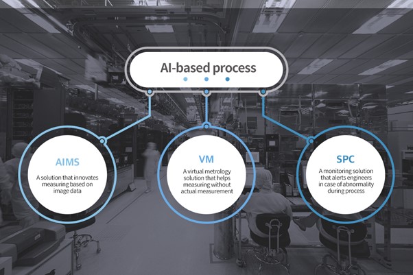
Gauss Labs is currently developing three solutions; Automatic Image Metrology for Semiconductor (AIMS), Virtual Metrology (VM), and Statistical Process Control (SPC).
AIMS is a solution that innovates metrology based on image data. In semiconductor manufacturing, the size of the circle and the level of damage is checked using electron microscopes to find defects. SK hynix generates millions of image data every day. AIMS uses computer vision (technology that builds human visual systems using certain algorithms) to enhance image quality and automatically take measurements, enabling faster and more accurate measurement. This will help semiconductor companies save costs since measuring equipment is extremely expensive.
Virtual Metrology (VM) is a solution that enables measuring without actually measuring. It uses equipment’s sensor data, which is generated when wafers are processed, and provides engineers an estimated measurement. This is especially useful for monitoring the condition of equipment and process. Applying a VM solution can save costs on equipment investments and maximize the efficiency of existing measuring equipment. Gauss Labs’ goal is to enhance the capability of VM so that it can completely replace actual measuring.
Statistical Process Control (SPC) is a monitoring solution that analyzes the probability of a problem occurring in each process or equipment with the help of machine learning and quickly lets engineers identify the cause of the problem. This root cause analysis can minimize simple repetitive tasks, significantly reducing equipment downtime (time during which a machine is not running) and allowing engineers to focus on solving core issues instead.
Gauss Labs expects the three solutions to generate economic effects worth hundreds of billions of KRW when fully applied in the overall manufacturing process.
“Our ultimate goal is to build an industrial AI platform by integrating all the solutions we develop. Applying the same solutions to different industries won’t be easy, but we will be able to easily apply the underlying technologies that make up the applications. We plan to build an open platform with the underlying technologies so that SK hynix and other semiconductor equipment, cloud service, and software companies can also freely participate and further develop, thus achieving innovation in industrial AI,” – Sunghee Yun, the Head of R&D.
How the Gauss Labs Works
Gauss Labs consists of two parts: the R&D organization that studies and develops AI solutions and the Program Management Office (PMO) that commercializes the AI solutions. The company has recruited the best experts in each area to strengthen its competency.
Sunghee Yun joined as Head of R&D. He comes from Amazon, where he built his expertise in AI technology through various fields including e-commerce after studying machine learning and convex optimization at school.

Sunghee Yun (Head of R&D)
The PMO organization is led by Moosung Kim, an experienced engineer who built his career at SK hynix and Intel. Kim is an expert in not only semiconductor manufacturing and equipment, but also AI through his experiences as a citizen data scientist.
Professors from prestigious Korean universities are also actively participating in Gauss Labs projects part-time in the fields of machine learning, statistics, control, vision, and scheduling. Gauss Labs is closely collaborating with various academics by attending related seminars by scholars at home and abroad; the company also plans to expand knowledge exchange programs in the coming months.
The R&D organization is divided into four teams in accordance with the technology they cover: CV/IP Team responsible for computer vision and image processing, ML/DS Team in charge of machine learning and data science, Operations Research & Engineering Optimization (OREO) Team, which focuses on planning and scheduling of the manufacturing process, and Software Architecture & Platform (SWAP) Team for development of software platform. Together, they analyze issues based on an understanding of the domain knowledge required to solve industrial AI issues and conduct research, development, and realization of AI algorithms using AI knowledge, intuition, and experience. The R&D organization also analyzes the latest AI technology trends to build a medium-to-long-term technology roadmap for Gauss Labs.
Moosung Kim, Head of PMO
The PMO organization designs products that customers need and manages projects. It must clearly define problems and issues at the manufacturing sites and communicate with AI engineers by converting the problems into mathematical language. As project manager and product owner, PMO must also set the direction for customers’ strategy in the long term.
Given the nature of industrial AI problems, even a single project requires a solution that integrates several technologies. Therefore, Gaussians are not bound to their teams but may instead work cross-functionally with other teams as a member of the same project under the matrix system for maximum synergy.
Gauss Labs also works closely with various relevant organizations, including SK hynix’s Manufacturing/Technology, Revolutionary Technology Center, and DT. Particularly, it’s working closely with SK hynix’s AI/DT Solution under Manufacturing/Technology and Data Architecture Team to jointly design the blueprint for a smart fab. To perform this project, they share data and domain knowledge needed in the development, monitor whether the solutions under development are appropriately applied at actual sites, and discuss key projects through regular meetings twice a week. Quarterly training that includes a fab tour is offered to Gauss Labs AI engineers to help them gain domain knowledge of the semiconductor industry.
“AI experts are not necessarily familiar with the domain, and domain experts don’t necessarily have a good understanding of how AI works. But in reality, you should know both to effectively apply the domain knowledge in building AI algorithms. We knew this would be a challenge for a team composed of only AI engineers. Furthermore, because Gauss Labs is not an internal team of SK hynix, it was very difficult to work closely together. So SK hynix created a counterpart team when Gauss Labs was born. Although SK hynix is our customer, we consider them as one team as we work together.” – Moosung Kim
Looking for new Gaussians to Join Our Journey
Gauss Labs is currently composed of 22 members and plans to more than double in size to 50 between the US headquarters and its Seoul office by the end of this year. Recruitment in the US, which has been inactive due to COVID restrictions, will begin in earnest starting June.
What capabilities and qualifications would Gauss Labs want from job candidates? And what would be a good reason for AI engineers to choose Gauss Labs, among others? CEO Mike shared his ideas and vision with Newsroom.

Mike Young-Han Kim, Gauss Labs CEO
Q. What makes the combination of AI and semiconductors attractive?
There is no other industry that generates as much data as the semiconductor industry. Being able to deal with real data generated from actual manufacturing sites will be a valuable experience for any AI engineer. Also, the opportunity to collaborate with frontline employees on real problems and data on-site is not easy to come by if you’re working for any startup. You will find several issues that are hard to address but worth exploring from the semiconductor manufacturing process. Another factor is that you will be able to achieve enormous economic impact through the solution you help create.
Q. What are the capabilities and qualities required from a Gauss Labs engineer?
Gauss Labs is walking a road not taken before and must deal with problems that are unsolvable with existing AI technology. We’re the ones who will define the problems to solve, creatively apply new forms of algorithms and insights to the problem’s core, and consider technologies from multiple angles. In short, we need engineers who are willing to face various challenges and bring innovative solutions.
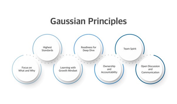
Gauss Labs refers to its principles when hiring new talent. The ‘Gaussian Principles’ define seven core values; Focus on What and Why, Highest Standards, Learning with Growth Mindset, Readiness for Deep Dive, Ownership and Accountability, Team Spirit, and Open Discussion and Communication. We are looking for talents who manifest these principles.
Q. What benefits would a Gauss Labs AI engineer gain?
The two hottest keywords today are AI and semiconductors. These two are the most important technologies that could change the fortune of a nation and provide the future growth engine in the era of the fourth industrial revolution. So anyone who has built a career at Gauss Labs, dealing with AI and semiconductors, will eventually mature into one of the most sought-after talents in the world. In addition, such experience will not limit the engineer to the semiconductor industry but will provide a foundation that will allow the engineer to expand to other industries.
Q. Any message for AI talent who wish to join Gauss Labs in the near future?
There’s no Google, Microsoft, or Amazon in the industrial AI area. It will be a tough journey, but the opportunity to become the world’s top player exists. Don’t miss the chance to advance in this field. Gauss Labs already has many talented engineers working to becoming the best in industrial AI, and we’re waiting for more to join our journey. There is much to learn here as an AI expert. We look forward to working with new AI talent with us soon.