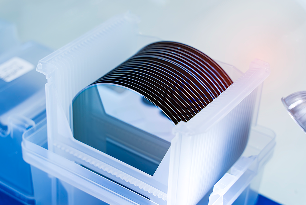
In semiconductor manufacturing, even the tiniest speck of dust can have a fatal impact on the electrical properties of the integrated circuit. If a pollutant generated in the process falls on top of a wafer or if small bumps are created on the surface of a wafer, this can cause a defect in the chip, lowering yield and dropping cost competitiveness. The more semiconductor circuit line width is reduced with scaling, the more intricate it becomes for the level of dust that can be permitted. ‘Defectless wafer’ that is clean, smooth and without a speck of dust is an essential element that determines product competitiveness.
Our newsroom met with the members of CLEAN & CMP Technology under the Manufacturing Technology department who are responsible for the production of ‘defectless wafers’ to learn more about their work.
Cleaning & CMP Process: Cleaning and Planarizing Wafer Surface
A wafer goes through various processes, including photo, etching, diffusion, and thin film, before becoming a complete semiconductor. Among these processes, the cleaning process physically or chemically removes pollutants on the wafer surface before and after different steps in the processing. Methods can be largely categorized into ‘wet cleaning,’ which uses chemicals, and ‘dry cleaning,’ which uses gas like plasma.
In the past, the cleaning process was considered as an auxiliary process under another processes, but it has recently become an essential key process necessary in producing reliable semiconductors. As circuit line widths reduced with increased degree of integration among elements, it became essential to further advance the way of controlling defects in wafers. Therefore, there is an increasing trend in rising importance of the cleaning process in removing residual foreign substances after various processes.

If the cleaning process is about cleaning wafer surface, the Chemical Mechanical Polishing (CMP) process is a process of smoothing the surfaces of wafers. The CMP process refers to the process of planarizing wafer surface by polishing the film surface of wafers that has bumps using a combination of chemical or mechanical forces.
This process uses the mechanism where areas of the chip of different heights are polished under different pressures when it comes into contact with a CMP pad, making the area that is relatively bumpier planarized first under a higher pressure. A chemical slurry is used on the surface in conjunction to prevent any scratches on the surface and to complement any instability in the process control.
Due to reduced line width following recent technological advancements, the degree of uniformity has gained more importance than before in the photo process. Similar level of defects has now a bigger impact on more cells, causing an even bigger drop in yield. As a result, the role of the CMP process of removing any irregular topography on the wafer surface is expanding. The process is gaining more significance in post-process stabilization by not only planarizing the surface, but also improving wafer defect, contributing to improving yield. Due to its even greater importance, every time a device is upgraded, the number of required CMP processes is increasing with even stricter standards.
Vision of CLEAN & CMP Technology: “Best Quality through Stabile Production and Technology Innovation”
There are eleven teams associated with the CLEAN & CMP process: Icheon FAB and Cheongju FAB have both Cleaning Technology Team and CMP Technology Team, which take charge of the cleaning process and CMP process, respectively. C&C Technology Innovation Team, which plays the role of a steersman in standardizing duties per fab and setting forth the overall direction for the organization, as well as the C&C Response Engineering Team, which oversees process dispersion improvement and endurance management of each fab.
The Cleaning Technology Team adopts and applies different methods such as the ‘batch-type’ cleaning1 or the ‘single-type’ cleaning2 out of wet cleaning methods according to the device and process. Because key parameters that determine the concept and endurance of equipment differ, the cleaning process is performed based on a deep understanding of both directions. In addition, the process is performed by choosing the right chemicals that will effectively remove defects according to the types and properties of the wafer defect.
A cleaning process that uses chemicals causes various defects due to the surface tension of the liquid chemical. The Cleaning Technology Team is dedicated to ensuring competitiveness by introducing ‘supercritical cleaning process’ that uses supercritical fluid that has no surface tension to control and further advance the process. The team is also gradually converting batch-type cleaning processes, which are hard to control with precision, into single-type processes.
The CMP process is performed by two parts – the polisher part and the cleaning part. In the polisher part, the slurry is injected onto the surface of the wafer and pad to polish off the wafer surface. And in the cleaning part, wet cleaning is performed using a brush to remove any residual substances left on the wafer surface after polishing. The process also includes a drying process after cleaning.
With circuit line width becoming more miniaturized, improving dispersion is also becoming more important to ensure process margin in the CMP process as well. The CMP Technology Team uses an Advanced Process Control (APC)3 system to optimize process conditions in real time. However, previous APC models were set based on the experience of the engineer in charge, meaning that improvements were influenced according to the skills and capabilities of the individual. Therefore, the CMP Technology Team recognizes the importance of developing an algorithm-based APC and a model that can leverage the experience of the engineer. It is implementing improvement measures of applying Model Integrated Process Control Optimizer (MICO) to further advance APC. The team is also focused on improving durables that can improve CMP Scratch (CMSC) defects generated in the CMP process.
The common objective pursued by CLEAN & CMP Technology is ‘ensuring the best quality through stabile production and technology innovation.’ To achieve this, members pursue four core values of ‘safety,’ ‘communication,’ ‘happiness,’ and ‘One Team Spirit.’ CLEAN & CMP Technology is dedicated to improving productivity and technology with a priority on ‘safety’ first and foremost due to the nature of processes that handles numerous equipment and materials.
Pointers from our CLEAN & CMP Technology Engineers

Jin Soo Kim, Technical Leader at DRAM Cleaning Technology Team
Q. Please tell us about your job.
Jin Soo Kim, Technical Leader (TL)
I’m an equipment engineer at DRAM Cleaning Technology Team. I am in charge of preventative maintenance, management, improvement activities and responding to various defects in cleansing equipment.
Min Hyuk Choi, Technical Leader (TL)
As a process engineer at DRAM Cleaning Technology Team, I identify causes of various issues that occur during the cleaning process and find solutions to the issues.
Chan Bum Park, Technical Leader (TL)
The CMP Technology Team largely oversees tasks related to either the process or the equipment. Among these tasks, I oversee the overall duties related to the process. I am in charge of yield, quality, productivity, and improvement activities.
Hye Bin Kim, Technical Leader (TL)
As a process engineer at DRAM CMP Technology Team, I optimize and manage the process for stable and reliable production. I also implement various assessments to improve and enhance yield and productivity. In addition, I analyze relevant data and make improvements in case issues or problems occur.
Q. Could you introduce some competencies your job requires?
Jin Soo Kim, Technical Leader (TL)
There are many instances where inflection points in the hardware that were unrecognized before cause a butterfly effect leading to process incidents of massive scale as the level of complexity of the process increases. Therefore, the role requires a critical mind and awareness of even the smallest details. The role also requires a comprehensive perspective and analytical abilities to identify issues with a multifaceted approach.
Min Hyuk Choi, Technical Leader (TL)
Collaborating with equipment and device engineers is critical for process engineers, and therefore an advanced level of interpersonal skills is essential.
Chan Bum Park, Technical Leader (TL)
Most of the work involves analyzing data captured in the process and from equipment to solve issues, which requires accurate analytical ability. The job also requires a wide perspective that can see issues from a comprehensive spectrum of aspects because equipment don’t always operate under same circumstances.
Hye Bin Kim, Technical Leader (TL)
In many cases, my job involves communicating with not only members from our team, but also with other teams and stakeholders. Therefore, good communication skills are important. Managing the process that has numerous variables requires a meticulous approach and accurate analytical skills. The role sometimes demands fast decisions to be made in case issues occur, and therefore, the ability to make accurate analysis based on data is very helpful.

Min Hyuk Choi, Technical Leader at DRAM Cleaning Technology Team
Q. What challenges have you encountered and how did you overcome them?
Jin Soo Kim, Technical Leader (TL)
The chance of actually checking a defect in an equipment and identifying the cause of the problem is extremely limited, thus it requires a process of conducting assessments in various ways to continuously narrow down on the cause of the issue. I also aim to come up with solutions by looking at the problem from a wide range of perspectives by leveraging collective intelligence rather than struggling with the issue alone.
Min Hyuk Choi, Technical Leader (TL)
Many times, it is difficult to identify the cause of process issues and come up with solutions alone. I communicate with other engineers and share thoughts and ideas to identify points of improvement to find the right solution.
Chan Bum Park, Technical Leader (TL)
Because of the nature of semiconductor manufacturing, having to explore and solve for an area with no visibility is the biggest challenge most members face. And the characteristics and features of fabs are all different, making it difficult to establish ‘One Fab.’ To overcome this, building a trusting relationship with relevant teams and stakeholders is crucial. We strive to think from a larger perspective from an organization and company’s point of view, beyond just our team.
Hye Bin Kim, Technical Leader (TL)
Due to the nature of the complexity in semiconductor processing, in many cases, there are times when there is more than just one cause to an issue because of the connectivity between different processes, the diversity of parameters, and time change. So, it is sometimes frustrating when there seems to be no clear one solution. There are times when I get stuck on the first hypothesis or a certain conclusion even while looking at the data. And the advice from close colleagues was what helped me solve the issue. I am also studying a statistics program to have a deeper understanding of data analysis while actively leveraging in-house training programs such as mySUNI (SK Group-led learning platform for employees) and SKHU (SK hynix University, integrated job competence training system) to improve my understanding of the overall semiconductor process.

Chan Bum Park (left), Technical Leader at C&C Technology Innovation Team
Q. What are the fascinating aspects of your work?
Jin Soo Kim, Technical Leader (TL)
It is very rewarding when we solve a difficult problem by digging into the problem to the end. Equipment don’t lie. If there is a phenomenon, there is a definite cause of the problem. I think that is the biggest appeal in working with equipment and device. The pleasure you feel when you’ve decided on an approach based on gathered data and assessment results and you find out that the approach was the right approach is the privilege only equipment engineers can enjoy.
Min Hyuk Choi, Technical Leader (TL)
It is the most rewarding when I’ve cleared a process issue or when the improvement measure has effect. Being able to share various thoughts and ideas with other engineers through collaborating and learning things I haven’t thought of from others is also another attractive part of the job.
Chan Bum Park, Technical Leader (TL)
They were different every year. In my first year, it was exciting to learn new things. After that, it was rewarding when I identified solutions to a number of variables in a difficult problem and made improvements to solve them. Now, I feel rewarded when I have the chance to widen my perspective by communicating with both senior and junior members and as I create an atmosphere where the whole team can work efficiently through solving issues by identifying what my team needs.
Hye Bin Kim, Technical Leader (TL)
I feel a sense of accomplishment when I apply an improvement measure to solve an issue and see that my approach improves dispersion and yield after a feedback process. Of course, there are times that I didn’t get the results I aimed for, but there is beauty in the process of finding solutions.

Hye Bin Kim, Technical Leader at DRAM CMP Technology Team
Q. What’s the atmosphere of the team like?
Jin Soo Kim, Technical Leader (TL)
Most issues that occur in the semiconductor process cannot be regarded as only an issue of the process or the equipment. Therefore, working with other engineers is extremely important. We make time to freely discuss issues and find effective solutions by enabling all members to communicate regardless of their years on the job or career experience. We manage our team under an ‘One Team’ system where there is autonomy in sharing thoughts and ideas but there is a clear structure and standard when it comes to making decisions or taking procedures.
Min Hyuk Choi, Technical Leader (TL)
Our team is horizontal and young. All members respect each other’s thoughts and communicate together regardless of work experience or years on the job.
Chan Bum Park, Technical Leader (TL)
We are dedicated to continuously improving our work environment through change and innovation. CLEAN & CMP organization gathers the thoughts of its members to build a happy and healthy environment and makes efforts to build a culture that fits each team’s characteristics based on the ideas of members.
Hye Bin Kim, Technical Leader (TL)
While it is a semiconductor fab that runs 24/7, there is a culture of recommending flexible work hours. It enables individuals to efficiently manage their time and it also helps us to refresh, which then improves overall work efficiency. We also actively support each other and collaborate on challenges and frequently share solutions or knowhows.
1A process that cleans several sheets of wafers by dipping them in a tank filled with chemicals. It costs less and can process many wafers per unit of time but is inappropriate to use in cleaning delicate and advanced wafers.
2A process that cleans one wafer at a time in each chamber inside the device using chemical solution. It enables a more precise control in the process but is expensive and the device itself is highly complex.
3A system based on a control and abnormality identification algorithm based on wafer measurement and processing model that adjusts conditions by identifying regularity using previous process tendencies or past data.