Hundreds of processes take place when making wafers into semiconductors. Among them, one of the most essential is etching. This process sees micro-patterns carved onto wafers by shaping circuits. For a successful etching process, it is important to manage the various variables within a set distribution and prepare each piece of equipment to operate in optimal condition. Our etch process engineers operate the manufacturing technology that handles this detailed work.
The SK hynix Newsroom team spoke with employees from the Icheon DRAM Front Etch, Middle Etch, and End Etch technology teams to learn more about their work.
Etching: Journey to Productivity Improvement
In semiconductor manufacturing, etching refers to engraving patterns on the film. The patterns are coated with plasma to make the final profile for each step of process. Its primary purpose is to accurately implement exact forms according to the layout, keeping results uniform and consistent under any conditions.
If a problem occurs during the deposition or photo processes, the problem area can be removed through selective etching. Alternatively, once something in the etching process goes wrong—it cannot be reversed. This is because it is impossible to refill the same material in the carved area. Therefore, etching is crucial in semiconductor manufacturing to determine the overall yield rate and product quality.
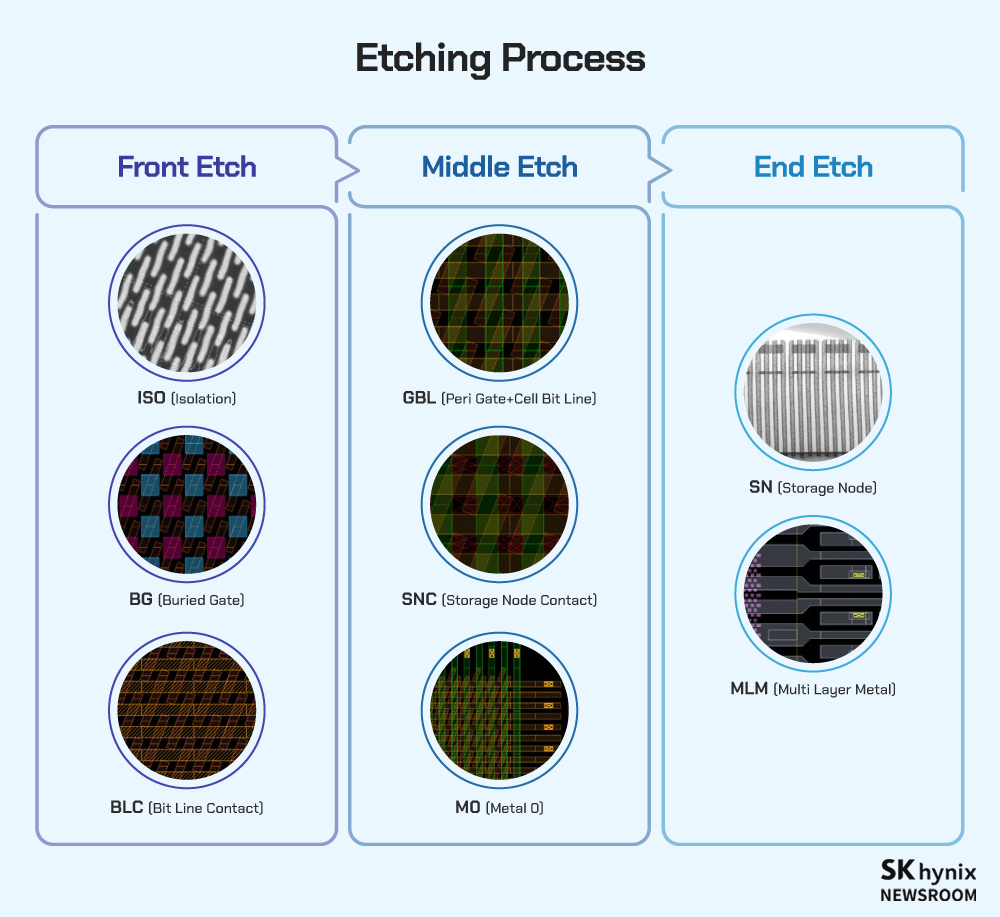
The etching process is comprised of eight steps: ISO, BG, BLC, GBL, SNC, M0, SN, and MLM.
First, the silicon (Si) of the wafer is etched in the ISO (Isolation) stage and the active region of the cell is created. During the BG (Buried Gate) step, the word line1 and gate are formed to make a channel for electrons. Next, connections between the ISO and bit line2 are created in the cell region during the BLC (Bit Line Contact) process. The bit line of the cell is created simultaneously with the gate in peri3 during GBL (Peri Gate + Cell Bit Line) process.
In the SNC (Storage Node Contact) phase, work to build connections between the active region and the storage node4 proceeds. Later, the connection point of S/D (Source/Drain)5 in peri, and between the bit line and storage node, is formed in the M0 (Metal 0) step. The whole process is complete once the capacity of the cell is confirmed in the SN (Storage Node) stage and the external power and internal wiring are created during MLM (Multi-layer Metal) phase.
As etch technologists are responsible for patterning semiconductors, the department is divided into three teams: Front Etch (ISO, BG, BLC), Middle Etch (GBL, SNC, M0), and End Etch (SN, MLM). The teams are also divided into manufacturing and equipment roles.
The responsibility of manufacturing roles is to manage and improve the unit production process. Manufacturing roles are essential for increasing the yield rate and improving product quality through variable control and other production optimizations.
Whereas equipment roles manage and enhance production equipment to avoid errors during the etching process. The core responsibility of equipment roles is to ensure the best performance of machinery.
Although separated by responsibility, all teams have the same objective—managing and improving the production process and relevant equipment to enhance productivity. To achieve the goal, each team shares their results and points of improvement, collaborating for better business performance.
How to Solve the Challenges in Miniaturization
SK hynix began mass production of 1anm 8Gbit LPDDR4 DRAM using EUV equipment in July 2021
Semiconductor memory’s circuit patterns have reached a level of 1anm and have been refined to accommodate approximately 10,000 cells in a single DRAM. As a result, the process margin proves insufficient even in the etching process.
When the hole6 is formed too small, a “not open” status can occur which blocks the lower portion of the chip. Alternatively, “bridge” phenomenon can become a problem when the hole is too large. “Bridge” phenomenon occurs when the gap between two holes is insufficient, and thus, they stick to each other in subsequent steps. As semiconductors become finer, the possible values of holes able to avoid these risks narrows gradually.
To solve this problem, etch technologists are continuing to make improvements including modifying the process recipe and APC7 algorithms as well as introducing new etch technologies like ADCC8 and LSR9.
Another challenge emerging, as customer needs become more diverse, is the trend of multi-product production. To meet such requirements, optimized process conditions for each product should be set separately. This presents a unique challenge as engineers must secure mass production technology that satisfies both prepared conditions and diverse ones.
For this, etch engineers introduced an “APC offset” 10 technique to manage various derivatives based on the core product, while building and utilizing a “T-index System” to manage products in an integrated way. These efforts are improving the system to suit multi-product production.
Let’s hear from our Etch Process Engineers.


What skills are required to complete the work done by your team?
Hana Kim, Technical Leader (TL)
I’m in charge of evaluating the work to improve dispersion as well as increase yield and productivity based on measured data by production engineers. Since etching is carried out with a hard-mask11 made through various linkage processes, meticulous and accurate analysis is required. The final pattern must be determined in the etching process, therefore it is important to respond quickly when changes occur in linkage processes. Accurate analysis of data related to the overall understanding of semiconductor production is key to forming a complete pattern.
Taehee Yoo, Technical Leader (TL)
As an equipment engineer, I’m in charge of the maintenance, repair, set-up, and removal of equipment. The most important job of an equipment engineer is maintaining equipment so production can proceed under optimal conditions. It would be nice if machines always operated consistently, but their condition changes from time to time based on numerous variables. Therefore, it is necessary to have a broad perspective and to be able to assess problems from multiple angles.
How do you continue to develop your expertise?
Minho Kim, Technical Leader (TL)
Being familiar with the latest technologies is important—but these days, so is data utilization. It’s necessary to find correlations between data points like equipment data generated during production and response data that appears as a result. So, I’m studying statistical theories to use in analysis.
Louis Lee, Technical Leader (TL)
Considering the nature of technical manufacturing work, stable production is considered a job well done. So, I check everything carefully. Since process technology and equipment technology are mutually compatible, you need to understand the production process but also have an overall knowledge of the equipment. Therefore, I keep studying equipment-related content during my spare time. Our team offers opportunities to rotate between process and equipment roles to help members increase their knowledge of both disciplines.
What do you find rewarding about your work?
Hana Kim, Technical Leader (TL)
It is rewarding when the yield rate is enhanced through changes in production conditions. Although I’m proud that etching is a core step which directly connects to yield rate, I sometimes feel pressured by the thought that even small mistakes can be critical to the yield. I guess that’s why it feels rewarding to safely hand over a quality wafer to the next step in production.
Louis Lee, Technical Leader (TL)
The etching process is sometimes referred to as the pinnacle of semiconductor production, as it often determines the yield rate. Therefore, I find solving each and every task rewarding. That is the charm of this work, feeling rewarded when I break through difficulties and solve problems. I also feel the same amount of pride when I positively influence other coworkers by sharing an improvement to the process.
How about the overall work atmosphere in your team and group?
Taehee Yoo, Technical Leader (TL)
We are all proud to be on this team as etching is complicated and accounts for a large part of the entire semiconductor manufacturing process. Everyone is dedicated to their work which creates a dynamic and lively atmosphere. This sort of positive workplace stems from the fact that our team values enjoying our personal time too—so naturally our work-life balance is great.
Minho Kim, Technical Leader (TL)
We have a horizontal company culture, so everyone can actively express their opinions. Of course, when it comes to the work, it’s intense, but our team atmosphere is all about caring and having respect for each other. The FAB operates 24/7, so the scope of work we’re responsible for is broad. This means sometimes our work-life balance can take a back seat, but because we genuinely respect each other and communicate well as a team, people go the extra mile to help each other keep a good balance.
1Word Line: a line, connected to the source portion of a transistor, responsible for reading and writing.
2Bit Line: a line passing though the transistor gate. When a voltage above a certain level is applied to the line, the transistor is turned on and is ready to read or write data.
3Peri: a peripheral circuit that controls cell operation.
4Storage Node: the sector managing data storage in DRAM, especially the lower electrode of the dielectric for data storage
5S/D (Source/Drain): source to emit electrons and drain to receive electrons.
6Hole: the level of empty electrons generated by the movement of electrons in a valence band.
7Advanced Process Control: a program that automatically adjusts variables per production according to a set calculation.
8ADCC (Active DC Control): a function to control the interrelationship determined by the RF Time through varying DC controller.
9LSR (Lam Spectral Reflectometer): a method to adjust the etching amount by calculating and estimating etching depth based on the reflection angle of light shot at the center of wafer.
10APC Offset: an automatic program to follow variables with a certain standard based on response performance for each product focusing on a certain product (usually a core product).
11Hard-mask: a material with high etching selectivity used before depositing photoresist as it is hard to exclusively etch the lower part with insufficient margin provided by photoresist alone.