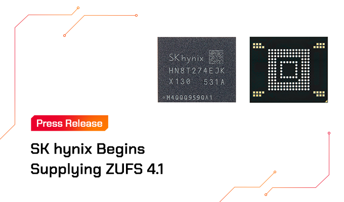
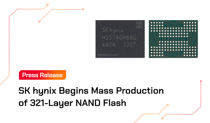
With a series of new high-spec products recently released by major smartphone manufacturers such as Apple, Huawei, and Xiaomi, the demand for high-capacity storage devices is booming. SK Hynix is leading the way in this space, presenting the world’s first ‘128-layer 4D NAND Flash’ and putting it into mass production in the second half of 2019 to industry-wide acclaim. This 128-layer NAND will soon be applied to next-generation storage devices for capacity that goes beyond 1TB, including Universal Flash Storage (UFS) and Solid State Drive (SSD). With this recent development, the launch of a 5G smartphone that possesses 2TB capacity is just on the horizon.
Industry-leading Capacity with the Highest Density has been realized

In June 2019, SK hynix succeeded in developing and mass producing the world’s first 128-layer 1Tbit Triple Level Cell (TLC) 4D NAND Flash.
This 128-layer NAND Flash is a TLC, the industry’s main product accounting for more than 85% of the NAND market, and currently holds the industry’s highest capacity of 1Tb. While other companies have developed 1Tb NAND products by building up a 96-layer Quadruple Level Cell (QLC), SK hynix is the first to commercialize the ultra-high-capacity NAND through TLC, achieving better performance and faster processing speed than QLC.
This exclusive SK hynix product also offers record-breaking vertical stacking that amounts to more than 360 billion NAND cells, each of which stores 3 bits per chip. Compared to existing 96-layer 4D NAND chips, a same-sized chip has 30% higher storage capacity, while reducing data read and write speed by 16%. What’s more, it also increases bit productivity per wafer by 40%, and the investment cost that comes with transitioning from 96-Layer to 128-Layer NAND has been reduced by 60% when compared to previous notable technology migrations.
Achieving a Next-gen Upgrade in just Eight Months
Representing a big step forward in the sector, this achievement took only eight months to develop from the time 96-layer TLC 4D NAND, its predecessor, was introduced. In October 2018, SK hynix succeeded in developing the world’s first Charge Trap Flash (CTF) based 4D NAND Flash* platform.

This innovative platform is how SK hynix significantly reduced the time required for developing new products to just eight months. Maintaining the same platform utilized for the 96-layer 4D NAND process, SK hynix focused on core processes and design technologies essential to increasing layers, resulting in the product’s successful development in such a short time. This will also be used as the platform for 176-layer 4D NAND, which SK Hynix plans to develop further. Considered among SK hynix’s greatest successes where SK hynix secured the fundamental competitiveness in the NAND sector, it goes beyond simply improving the company’s production and investment efficiency.
Highly Applicable as a High-Speed, High-Capacity Storage
Utilizing the 128-layer 4D NAND Flash, SK hynix plans to launch various cutting-edge solutions from 2020.
During the first half of next year, SK hynix plans to develop a next-generation UFS 3.1 product fully compatible with 5G flagship smartphones. When utilizing this product, the number of NANDs required to make 1TB – the largest smartphone capacity to date – products possible, will be cut in half when compared to 512Gb NANDs. This makes for a mobile solution that consumes 20% less power and is 1mm-less thick. If 16 units of the 128-layer 1Tb 4D NAND are formed into one single semiconductor package, even a 5G smartphone of 2TB storage capacity – the largest ever in the industry – will be available.
Furthermore, SK hynix will start mass producing 2TB consumer SSDs with a built-in controller and software, during the first half of next year (2020). Based on its power efficiency, which is 20% more than the previous generation, 16TB and 32TB Non Volatile Memory express (NVMe) SSDs for cutting-edge cloud data centers optimized for AI and big data will also be released next year.


