As part of its development of next-generation 4D NAND flash products, SK hynix recently developed products with 238 layers, the world’s highest. This could be thought of as difficult as cramming 4 billion 238-story buildings onto a dime-sized area.
These miniature skyscrapers are what allow us to store all of our life’s memories and heavy workloads on PC storage devices and servers, as well as many other devices around us.
The newsroom looks back at some of the NAND breakthroughs SK hynix has produced to push the boundaries of technology while obtaining a market advantage and being acknowledged as an industry standard.
Increasing demand for high-performance NAND
An ever-growing demand for NAND has been the force driving behind SK hynix’s efforts to meet customer needs. Price is important as it always has been, but performance has become increasingly crucial in recent years.
Take digital cameras: they now have a huge number of pixels, and a memory capable of storing a large amount of data is required for just one image. Consumer demand for fast read and write speeds is also increasing as SSDs become more popular.
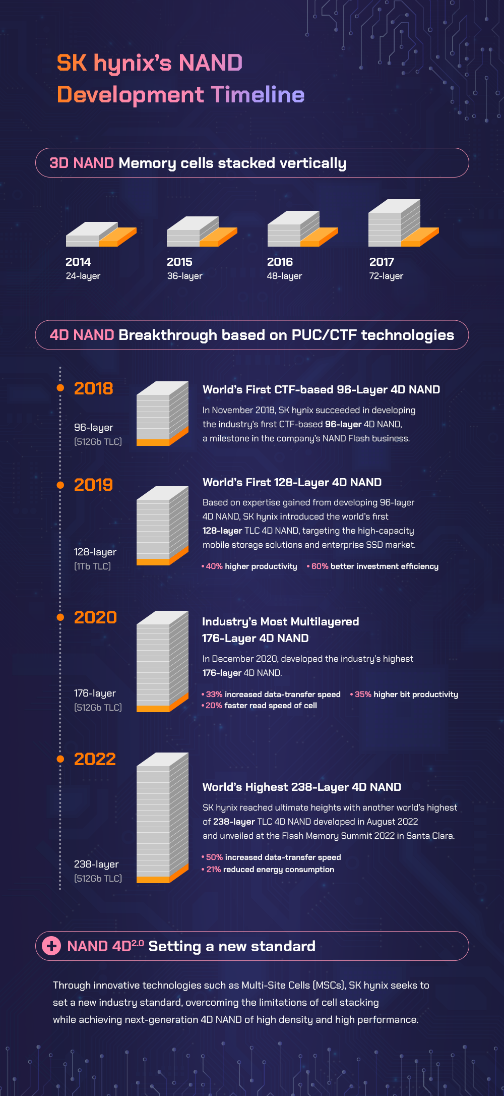
Until early 2010, the most pressing issue in memory technology was the scaling of 2D NAND, that is, making things smaller. However, due to limitations in density and fine patterning, 3D NAND became the focus of all manufacturers, including SK hynix.
3D NAND development history at SK hynix
3D NAND literally refers to the stacking of memory cells vertically. The bit density improves as more layers are added, increasing the storage capacity.
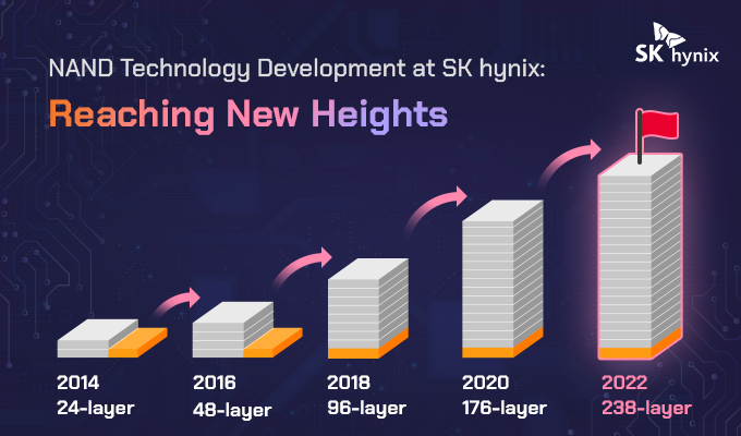
In November 2014, SK hynix was able to develop 3D NAND chips featuring 24 layers. Then, in August 2015, it developed 36-layer 128Gb 3D NAND based on its TLC arrays technology, followed by 48-layer 256Gb TLC in November 2016.
Just 5 months later, the company introduced the industry’s first and highest productivity 72-Layer 256Gb TLC 3D NAND, with 30% higher productivity and 20% higher performance than 48 layers, thereby establishing its business competency in 3D NAND memory solutions.
This was also a significant accomplishment given the importance of NAND memory in this new era of AI, Big Data, and Cloud storage.
Breakthrough from 3D to 4D NAND
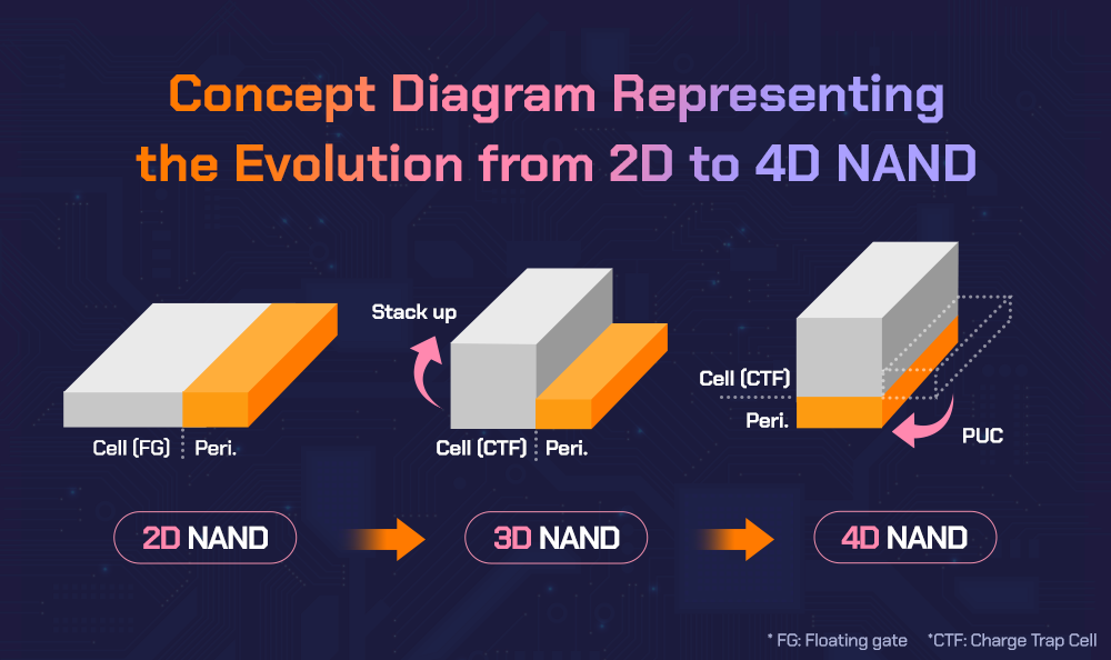
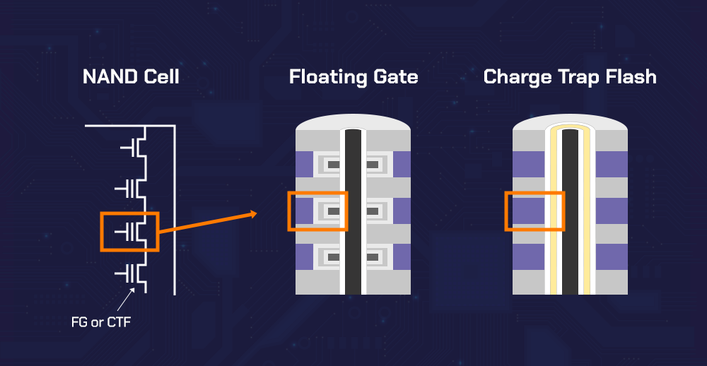
At SK hynix, it was also important to innovate 3D NAND and think outside the box. This included the development of PUC (Peri Under Cell), a technology that puts peripheral circuits, generally placed on the side, under cell circuits to reduce chip space, giving rise to 4D NAND. Two other core competencies that are applied to its 4D NAND products include Sideway Source, a technology that horizontally connects the source, and Advanced CTF, that stores electric charges in a CTF (Charge Trap Flash).
In November 2018, SK hynix achieved a major milestone in the company’s NAND flash business with the successful development of the industry’s first CTF-based 96-layer 512Gb TLC 4D NAND.
SK hynix then introduced the world’s first 128-layer 1Tb TLC 4D NAND, dramatically enhancing profitability with 40% greater productivity and 60% better investment efficiency, targeting the high-capacity mobile storage solutions and enterprise SSD markets.
In December 2020, the company developed the industry’s highest 176-layer 512Gb 4D NAND. In a recent quality evaluation survey of leading mobile device and SSD manufacturers, SK hynix’s 128-layer and 176-layer NAND products ranked first.
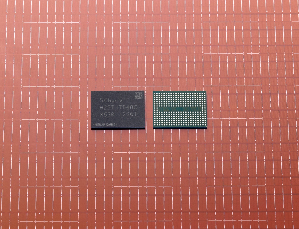
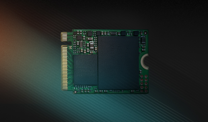
▲ Figure 2. SK hynix 238-layer 512Gb TLC 4D NAND
In August of 2022, SK hynix developed the world’s first 238-layer 512Gb TLC 4D NAND, which was introduced at the Flash Memory Summit 2022 in Santa Clara. Besides increasing productivity and data transfer rate, energy consumption for data reading is reduced by 21%, contributing to the fulfillment of ESG management goals.
Thanks to the dedication and tireless work of its developers, SK hynix’s current 4D NAND technology is now acknowledged as an industry standard.
NAND 4D2.0: Setting a new standard
Current 4D NAND reduces chip sizes thanks to PUC. While this allows the implementation of high density within a fixed area, the disadvantage is that the stacking technology may reach its limit in the future.
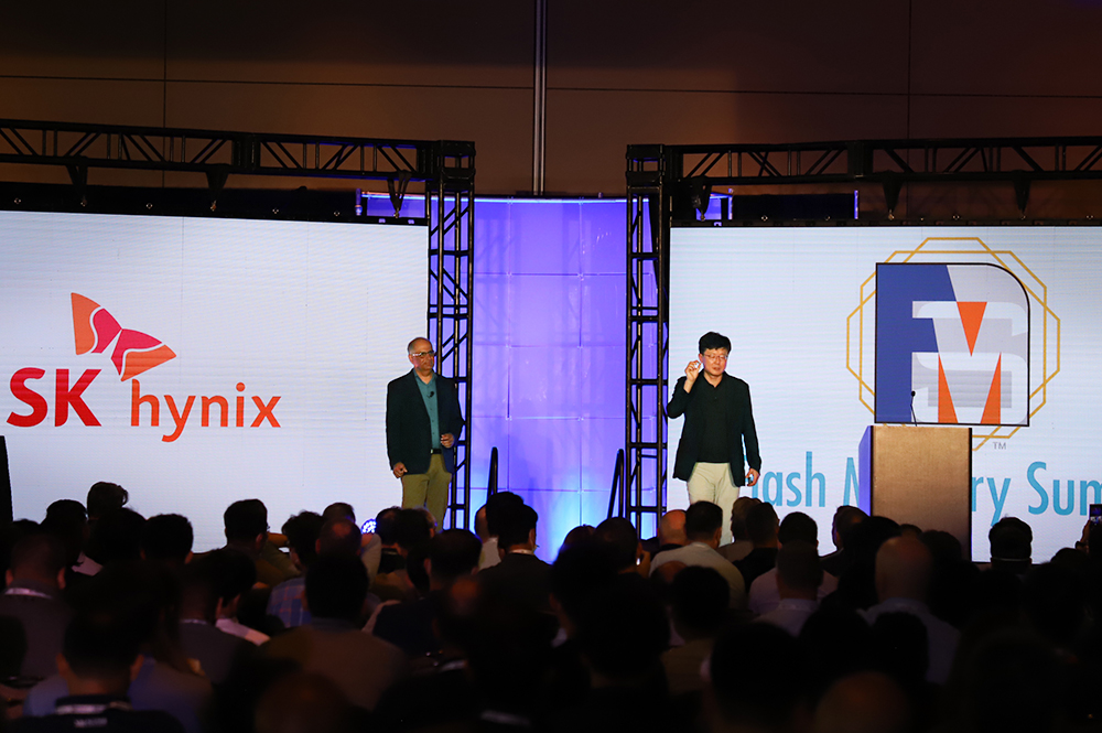
▲ Figure 3. Jungdal Choi, Head of NAND Development of SK hynix (right), delivers his keynote speech with Sanjay Talreja of Solidigm (left) at the Flash Memory Summit 2022
SK hynix plans to overcome this barrier by using Multi-Site Cells (MSCs) as the core, once again demonstrating its technological prowess ahead of others. These store data by dividing existing cells into two smaller cells with micro fabrication, reducing the number of cell stacks while horizontally expanding cell density, one of the core elements of the technological concept known as 4D2.0. Such disruptive technology is projected to become the industry’s next-generation standard.
Bold investments and foresight key to future success
As the NAND market has grown, so has SK hynix’s success in developing and mass-producing NAND solutions that are significantly different from conventional NAND, giving it a competitive advantage.
SK hynix has concentrated not just on stacking, but also on technological innovation and new ways of thinking, all part of the company’s long-term investment in R&D. By optimizing the arrangement of cells, SK hynix has been able to increase performance enough to meet the changing needs of customers.
Limitations will no doubt surface as NAND technology advances, but SK hynix is committed to delivering the industry’s best products while continuing to think outside the box and deliver new, timely, and differentiated technologies.