

With the development of information and communication technology (ICT), the amount of information that humans have accumulated over the last three decades is far greater than the amount of knowledge created over the past 5,000 years. This amount of information is doubling every three months, and as of 2020, it is estimated that the total amount of information generated by humans is 40 zettabytes1. In the future, the amount of information generated by ubiquitous computing2 such as big data, social networking services (SNS), Internet of Things (IoT), and cloud computing is expected to increase geometrically.
According to this trend, various electronic products including mobile devices are evolving in the direction of smaller (“ultra-small”), less power consumption (“ultra-low-power”), and “faster (ultra-high-speed”) products. Furthermore, combined with artificial intelligence (AI) or IoT, they are developing into intelligent devices.
To accumulate an enormous amount of information in a small area, semiconductor devices for storing or processing information are also becoming more miniaturized in a several nanometer level with higher density. As a result, the manufacturing process has become more complicated, and power consumption due to heat generation is also rapidly increasing.
Accordingly, there is a growing voice about the necessity of improving the existing semiconductor operation method which uses electron charge3 in order to reduce power consumption drastically. To achieve this, many technological developments are currently being made. Among the next-generation low-power semiconductor technologies developed until today, a technology called “spintronics”4 that uses electron spins5 is evaluated to realize ultra-low power.
This technology simultaneously uses two physical quantities6 of electrons, which are charge and spin, and is implemented in a way that the resistance of a device changes according to the direction of the spin. Therefore, the processing speed is fast and heat is not generated in the device when a current flows, which makes its power consumption very low. For this reason, the magnetic random access memory (MRAM) technology using the spin is expected to lead the growth of next-generation ultra-low-power information storage devices in combination with semiconductor technology in the future.
Principles and Limitations of the MRAM Technology at Early Stage
The core part of an MRAM is a magnetic tunnel junction (MTJ) located at the intersection of a digit line7 and a bit line8 of the memory circuit. An MTJ basically has a three-layer structure consisting of a fixed (magnetic) layer, a dielectric tunnel barrier, and a free (magnetic) layer. Here, a magnetic layer that can easily change the direction of magnetization9 is called a free layer, while a magnetic layer that is pinned so that the magnetization direction cannot be easily changed is called a fixed layer.
One of the key features of an MTJ is that the resistance of the device varies depending on the relative magnetization directions of the two magnetic layers. When the magnetization directions of the two magnetic layers constituting the MTJ are aligned in a parallel direction, the device has a low electrical resistance value. On the contrary, when they are aligned in an anti-parallel direction, the device has a high resistance value.
If the high resistance value when not parallel is defined as RAP, low resistance value when parallel as RP and the difference between the two values as ΔR (ΔR=RAP–RP), the magneto-resistance (MR ratio) can be generally defined as ΔR/RP. The MR ratio is determined depending on which magnetic material and dielectric tunnel barrier are used, and is usually divided by tens to hundreds of percent.
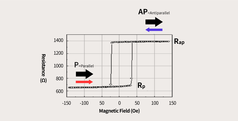
Resistance changes in MTJ according to changes in the external magnetic field in an MRAM
An MRAM stores information in “1” and “0” in the binary system by using the state of different RAP and RP when the magnetic field is 0. In the graph above, the x-axis represents an externally applied magnetic field and the y-axis represents the level of electrical resistance. When x value is 0 (x=0), RP and RAP show two different electrical resistances of 650 ohm10 and 1,400 ohm, respectively. By using this, RP is recognized as 0, and RAP is recognized as 1 to store information. Conversely, to read the information recorded in the MTJ, the resistance state of the MTJ should be measured.
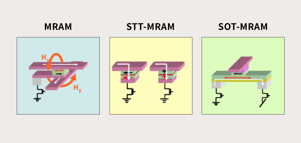
To store information at this point, the magnetization direction of the free layer in the MTJ should be changed. In MRAMs at an early stage, a current was flowed through the digit line to induce a magnetic field to change the magnetization direction of the free layer. As the degree of integration gradually increased, however, an interference phenomenon occurred in which information of adjacent cells was read, and energy required for changing the direction increased. For this reason, this method is no longer used with a limit of 64 kilobytes (KB).
Principles, Advantages, and Disadvantages of Spin-Transfer Torque MRAM (STT-MRAM) Technology
What has overcome such fatal disadvantage is the spin-transfer torque magnetic random access memory (STT-MRAM) technology. Unlike the conventional MRAM method that changes the magnetization direction of the free layer through generating a magnetic field by making a current flow in the digit line, STT-MRAMs use a method of making a current directly flow in the MTJ to change the magnetization direction of the free layer. What makes this possible is the spin-transfer torque (STT).
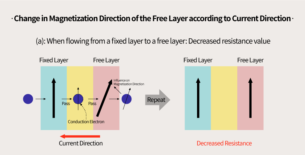
When making a current flow in the MTJ from the fixed layer to the free layer, the spin direction of the conduction electrons11 is aligned to the spin direction of the fixed layer (arrow direction in the figure above) due to the influence of the magnetic exchange coupling energy12 in the process where the conduction electrons pass through the fixed layer. At this time, the current in which the spins are aligned in one direction is called a spin-polarized current.
When this spin-polarized current enters the free layer, the interaction between the spin electrons inside the free layer aligned with the magnetization direction (diagonal arrow in the figure above) of the free layer and the conduction electrons flowing in a state aligned in the magnetization direction (vertical arrow in the figure above) of the fixed layer changes the spin direction of the conduction electrons just before and after passing through the free layer.
The time taken when the spin direction changes like this is called “torque”. When spin-polarized conduction electrons are introduced in the free layer and torque of a certain level or above is applied, the magnetization direction of the free layer can be changed to the same direction as that of the fixed layer, through which the information is stored. When the magnetization directions of the two magnetic layers are aligned in a direction parallel to each other, the device can have a low resistance value.
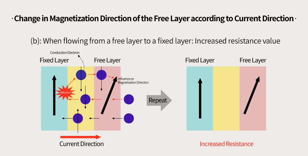
To delete the stored information, the magnetization directions should be changed from parallel to antiparallel. To achieve this, electrons should flow from the free layer to the fixed layer, contrary to the previous process. As seen from the right of the figure above, when conduction electrons move from the free layer to the fixed layer, electrons which have spins in the same magnetization direction as the fixed layer pass through the fixed layer, while electrons which do not are reflected back to the free layer. These electrons apply a torque in a direction opposite to the magnetization of the free layer and reverse the magnetization direction of the free layer, which makes it possible for the magnetization directions of the two layers to be aligned in an antiparallel state. At this time, the device has a high resistance value.
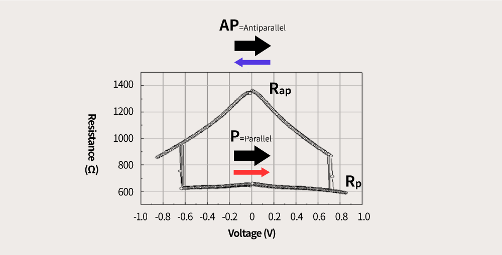
The resistance changes of the MTJ when applying a current
(application: the act of applying power voltage between terminals of an electric circuit) in an STT-MRAM
The figure above shows the magneto-resistance values measured while changing the magnetization direction of the free layer by making a current flow through the MTJ of an STT-MRAM. RP is 650 ohm and RAP is 1,400 ohm, which are the same as the measurement values in the conventional MRAM method that generates a magnetic field by making a current flow through the digit line.
To read the information stored in an STT-MRAM, what should be done is measuring the resistance of the MTJ, just like in MRAMs. The only difference between STT-MRAMs and MRAMs is the method of applying the current to record information. Through this, however, STT-MRAMs completely overcame the limitation of density and the interference phenomenon of adjacent cells, which were pointed out as disadvantages of MRAMs. For this reason, STT-MRAMs are recognized as a key technology to realize the next-generation non-volatile memory.
Principles, Advantages, and Disadvantage of Spin-Orbit Torque MRAM (SOT-MRAM) Technology
When a magnetic field is applied to a conductor through which a current flows, a voltage is induced in a vertical direction to the direction of the current and the magnetic field, and this effect is called the “Hall effect”. Also, the “spin Hall effect” refers to a phenomenon where the Hall effect appears in a material with a strong spin-orbit interaction (SOI) even without applying an external magnetic field.
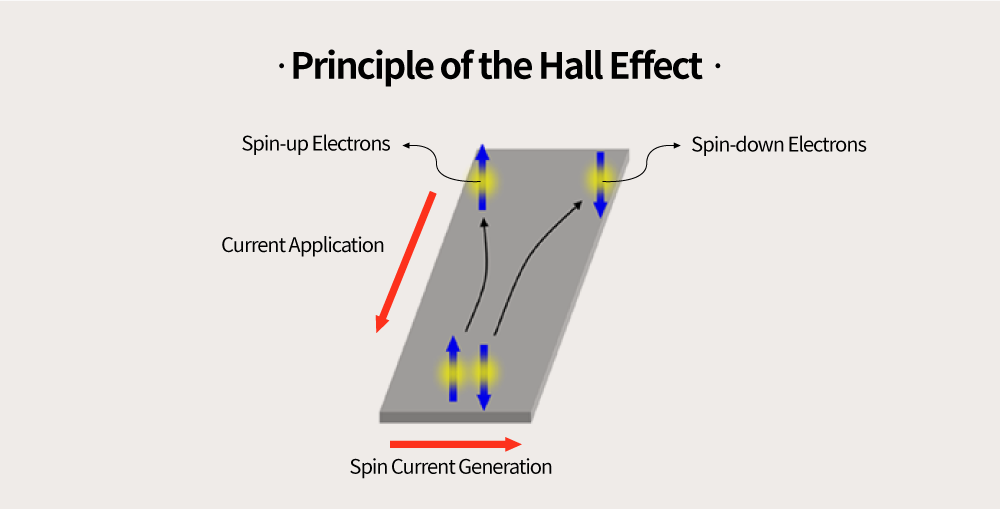
When a current is applied in the vertical direction to materials with a high SOI level such as tantalum (Ta), tungsten (W), and platinum (Pt), conduction electrons are separated into spin-up electrons with the upward spin direction (left in the figure above) and spin-down electrons with the downward spin direction (right in the figure above). At this time, a spin current in the horizontal direction is generated from the spin-up electrons to the spin-down electrons. At this stage, the spin current can be used to switch the magnetization direction of the free layer of the MTJ, and the memory which adopts this method is called spin-orbit torque MRAM (SOT-MRAM).
Comparison of circuit structure of MRAM, STT-MRAM, and SOT-MRAM
Unlike STT-MRAMs, where a current is directly applied vertically to the MTJ, SOT-MRAMs utilize a method in which the spin current polarized in the vertical direction by the spin Hall effect changes the magnetization direction of the free layer when a current is injected in a horizontal direction into a material layer with a high SOI level at the bottom of the MTJ cell.
In particular, when comparing to STT-MRAMs, SOT-MRAMs can generate more conduction electrons with the same spin and inject them into magnetic layers. This suggests a stronger torque and an easier switch of the magnetization direction of the free layer, which makes it possible to achieve a faster processing speed and lower power consumption.
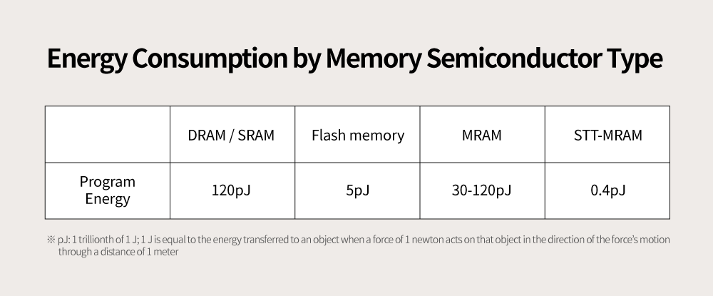
A table comparing energy consumption for programming 1 bit in each type of memory semiconductor
Assuming that a 90 nm process is used, a large amount of 120 pJ13 is used in a typical MRAM, while only 0.4 pJ of energy is consumed in an STT-MRAM. When using a process with a line width narrower than 90 nm is used, the gap between the two technologies is increased. This low-power characteristic of STT-MRAMs is very significant in terms of energy efficiency. Also, the power consumption of SOT-MRAMs is about a tenth of that of STT-MRAMs, which is expected to further reduce power consumption.
In the modern von Neumann computing technology architecture, there is a gap between the operating speed of the processor (0.1 ns14) and the operating speed of the main memory (10-100 ns) and the storage memory (0.1-10 ms15). To ensure that the next-generation memory technology is able to cover a wide area from cache16 to main memory, an operation speed of 1-10 ns is required. Among the currently available technologies for the next-generation memory semiconductor, STT-MRAMs (10 ns) and SOT-MRAMs (1-10 ns) are the only technologies that satisfy this requirement. Among these two, SOT-MRAMs have the lowest power consumption level, drawing attention as the optimal technology for the next-generation memory.
1 Zetta is a decimal unit denoting a factor of 1021 and a byte is a unit denoting the magnitude of data. The units increase in the orders of kilobyte (KB), megabyte (MB), gigabyte (GB), terabyte (TB), petabyte (PB), exabyte (EB), zettabyte (ZB), etc. Each time the unit is changed, the size of data increases by 1,000 times.
2 This refers to a computing environment in which computers and the Internet can be used anytime, anywhere. Ubiquitous is a term derived from the Latin word “ubique” which means “everywhere”.
3 A property or physical quantity (a quantity representing the property or state of a substance) of a substance that causes an electric phenomenon; each of all particles is positive (+), negative (-), or neutral.
4 Spin is one of the physical quantities representing the basic properties of a particle. As a particle’s inherent angular momentum (intensity or momentum of a rotary motion), it has a momentum level and direction. In addition to the motion of the electrons orbiting the nucleus, it rotates around an axis that passes its center of gravity, and this rotational motion is called a “spin”.
5 An electronic engineering technology in which data is stored by dividing the phenomenon of electrons rotating in different directions into two digital signals of 0 and 1
6 A quantity representing the property or state of a substance, described by length, weight, viscosity, mass, temperature, capacity, etc.
7 An electrical circuit for entering information
8 An electrical circuit for reading stored information
9 To induce magnetic properties into an object with no magnetic properties; the magnetization direction of magnetic materials is determined with the direction of N pole to S pole.
10 The unit of electrical resistance; 1 ohm is defined as the resistance of a mercury column of 1 mm2 cross-section area and 106 cm long.
11 Electrons that are not bound to any particular atom and can move freely
12 The energy that describes the magnetic interaction between adjacent spins; when the spin direction is the same as the direction of adjacent spins, the energy is low.
13 J is a unit of energy and 1 J is equal to the energy transferred to an object when a force of 1 newton (N) acts on that object in the direction of the force’s motion through a distance of 1 meter. The pJ, abbreviation of picojoule, is a unit that means 1 trillionth of 1 J.
14 nanosecond; a unit representing one billionth of a second
15 microsecond; a unit representing one millionth of a second
16 A high-speed memory device in the form of a buffer that is installed between the main memory and the central processing unit (CPU) to temporarily store commands or programs read into the main memory

ByDr. Joonyeon Chang
Director-General of Post-silicon Semiconductor Institute of KIST


