News Highlights
- Two joint academic papers on AI-based metrology technology presented
- Gauss Labs’s innovative technology improves process control and equipment productivity in semiconductor manufacturing
- Gauss Labs is at the forefront, leading industrial AI efforts to transform the manufacturing industry
Seoul, February 29, 2024
SK hynix Inc. (or “the company”, www.skhynix.com) and Gauss Labs announced today that they participated in the SPIE AL1 2024, an international conference held in San Jose, California, and presented two papers based on the latest technology for AI-based metrology.
1SPIE Advanced Lithography + Patterning (SPIE AL): A conference hosted by the Society of Photo-Optical Instrumentation Engineers (SPIE), the most prestigious international society in optics and photonics following foundation in 1955, where overall lithography technology for drawing semiconductor circuits are discussed
2Metrology: Measuring the physical and electrical characteristics to ensure that requirements are met in the manufacturing process
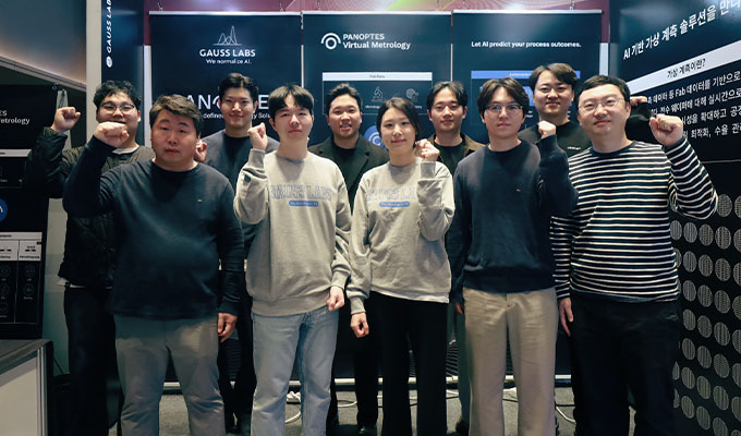
 poses with his colleagues")
Figure 1. Gauss Labs CEO Mike Kim(center) poses with his colleagues
SK hynix has been collaborating closely with Gauss Labs in various areas to increase semiconductor yield and productivity, and the results of this collaboration are published in these two papers.
In the paper “Model Aggregation for Virtual Metrology for High-Volume Manufacturing,” Gauss Labs introduces “aggregated AOM3“, an algorithm that increases the prediction accuracy of its AI-based virtual metrology solution, Panoptes VM (Virtual Metrology).
3Adaptive Online Model (AOM): Modelling algorithms that address data changes due to process state changes and maintain high predictability
Since its adoption in December 2022, SK hynix used Panoptes VM to conduct virtual measurements on more than 50 million wafers so far, which translates to more than one wafer per second. The company was able to improve process variability4 by 29% thanks to this technology.
4Variability: The scale of the quality variation of the products from a certain process. It is important to maintain a low process variability in order to keep the product quality consistent.
The latest algorithm by Gauss Labs, the aggregated AOM, pools processing machines, chambers, etc. that share the same pattern and models them together. According to Gauss Labs, this solves the challenge of data shortage while further increasing the prediction accuracy.
In its second paper, “Universal Denoiser to Improve Metrology Throughput,” Gauss Labs introduces a “universal denoiser”, which removes random variations (noise) from CD-SEM5 images. Measurements from CD-SEM images are taken at nanometer scale, so it is extremely important to remove noise in order to take measurements accurately.
5Critical Dimension Scanning Electron Microscope (CD-SEM): Equipment that combines electronic and infrared optical microscopes to measure the size, shape, and position of semiconductor patterns
Gauss Labs’s universal denoiser uses AI to remove noise from various types of images at once. Through a series of extensive tests with SK hynix, Gauss Labs observed image acquisition time reduced to as much as ¼, compared to conventional technology. Gauss Labs states that this technology is expected to improve the productivity of metrology equipment by 42%.
Mike Kim, CEO of Gauss Labs, said that his company is working on research and development for applications of industrial AI in real-world semiconductor manufacturing fabs. “We will continue to launch innovative AI-based solutions to revolutionize manufacturing.”
Authors
- Minsuk Shina, Minju Junga, Simon Zabrockia, Doh-Hyung Rob, Hyeon-Kyeong Jeongb, Dongkyun Yim a, “Model aggregation for virtual metrology in high-volume manufacturing,” SPIE Advanced Lithography + Patterning (2024)
- Yonghyun Kima, Seyun Kima, Hoon Byuna, Sang-Gil Parka, Tae Jong Leeb, Seong Il Leeb, Min Woo Kangb, Il Koo Kima, “Universal denoiser to improve metrology throughput,” SPIE Advanced Lithography + Patterning (2024)
aGauss Labs
bSK hynix
Disclaimer
These materials are not an offer for sale of the securities of SK hynix Inc. in the United States. The securities may not be offered or sold in the United States absent registration with the U.S. Securities and Exchange Commission or an exemption from registration under the U.S. Securities Act of 1933, as amended. SK hynix Inc. does not intend to register any offering in the United States or to conduct a public offering of securities in the United States.
About SK hynix Inc.
SK hynix Inc., headquartered in Korea, is the world’s top tier semiconductor supplier offering Dynamic Random Access Memory chips (“DRAM”), flash memory chips (“NAND flash”) and CMOS Image Sensors (“CIS”) for a wide range of distinguished customers globally. The Company’s shares are traded on the Korea Exchange, and the Global Depository shares are listed on the Luxembourg Stock Exchange. Further information about SK hynix is available at www.skhynix.com, news.skhynix.com.
About Gauss Labs Inc.
Gauss Labs develops innovative industrial AI solutions and software products to make factories more intelligent by leveraging machine-generated data. It was founded in August 2020 and now has two international locations in Silicon Valley, CA, and Seoul, Korea. Further information about Gauss Labs is available at www.gausslabs.ai.
Media Contact
SK hynix Inc.
Global Public Relations
Technical Leader
Sooyeon Lee
E-Mail: global_newsroom@skhynix.com
Technical Leader
Kanga Kong
E-Mail: global_newsroom@skhynix.com