Being stuck in traffic on a two-lane highway during the morning rush hour is most workers’ nightmare. With cars lined up bumper-to-bumper and nowhere to turn, drivers are forced to stay in their lane and slowly reach their destination. Similarly, data can get stuck in a traffic jam when only a few channels are tasked with transferring enormous amounts of data between processors. Especially in today’s data explosion era driven by the use of technologies such as artificial intelligence and supercomputers, the need for effective input/output (I/O) interface circuits that transfer data with high speed and minimal distortion has never been greater.
In this second episode of the series written by professors of Daegu Gyeongbuk Institute of Science and Technology (DGIST), Professor Gain Kim of the Department of Electrical Engineering and Computer Science will explain the features of I/O interface circuits. This article will cover how the circuits work, the use of different circuit architectures in modern systems, their various applications, and their evolution over the years.
Why are I/O Interface Circuits Important for Data Transfer?

Figure 1. Diagram showing the communication between chips carried out by a wired transmitter (TX) and a receiver (RX)
These electrical signals are essentially voltage information holding the binary numbers ‘0’ and ‘1.’ Although this might seem like simple information is being transmitted, it requires significant processing steps to transmit these 0s and 1s.

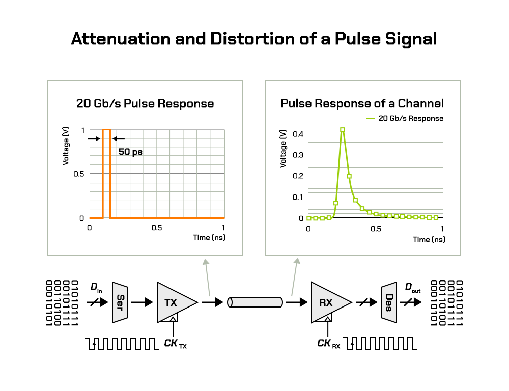
Figure 2. An archetypal pulse signal (single-bit) that experiences attenuation and distortion after passing through a wired circuit
One of the reasons for this lies in the fact that there is an enormous amount of output binary data that a processor must handle per unit time to ensure high-speed communication between chips. However, the number of pads that act as the pathway between the inside and outside of a chip is limited. As mentioned in the beginning, this is comparable to there being a large number of vehicles on a city highway with a limited number of lanes. If the number of data transfer channels is restricted like this, the flow of data in each channel—or metal wires—must be as fast as possible to transfer data without disruption. However, increasing the speed of data flow in a limited space of a channel will make it difficult to distinguish between the signals 0 and 1 when the data arrives at the other chip’s receiver. This is due to the signal experiencing attenuation (weakening) and distortion as it travels through the wire and reaches the receiver as in Figure 2. In general, there is a greater amount of attenuation and a higher degree of distortion to the signal the longer the wire gets. Taking these defects into consideration, it is the role of a circuit called an equalizer to restore the signal to its original form as much as possible.
What is the Role of an Equalizer?

Figure 3. A signal impaired by a wired channel is restored by the receiver’s equalizer (EQ) and shows a clear distinction between its 0s and 1s
The equalizer is divided into a transmitter that sends the data out to the wire and a receiver that receives the data from the wire. As for the signal that is restored by the equalizer, it will have a clear distinction between 0s and 1s again as shown in Figure 3. However, when the transmitter sends a 0 and the receiver reads it as a 1 or vice-versa, this misreading of signals is called a “bit error.” So, the equalizer reduces the occurrence of these bit errors—or the bit error rate. Transmitters and receivers that hold these functions are collectively referred to as a serial link, a wireline transceiver, or a SerDes (serializer-deserializer1). It is the combination of these serial links that then form an I/O interface.
1Serializer-deserializer (SerDes): A transmission system that sends signals over a high-speed connection from a transceiver on one chip to a receiver on another. The transceiver converts parallel data into a serial stream of data that is re-translated into a parallel form on the receiving end.
How Have I/O Interfaces Evolved?

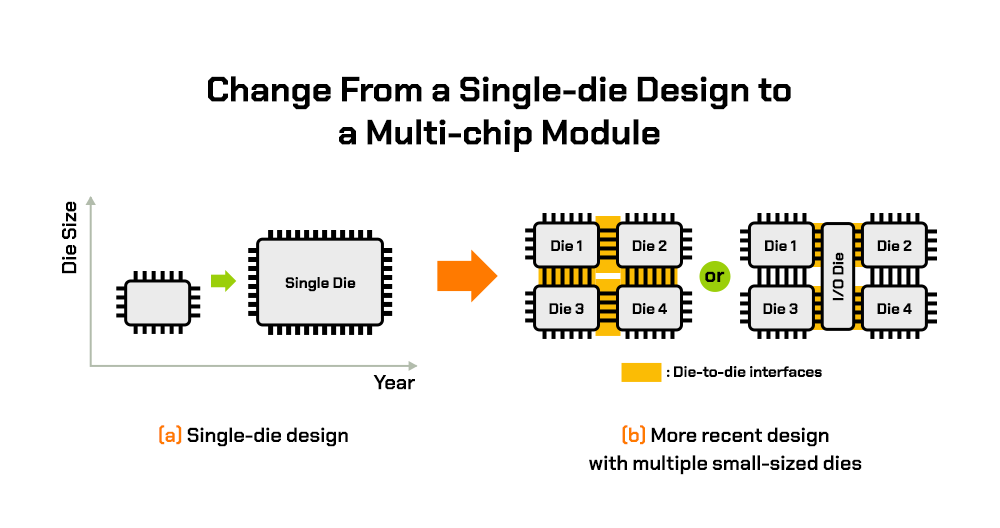
Figure 4. A comparison of the design of high-performance processors (a) in the past featuring a single die (b) and a more recent design with multiple small-sized dies
In recent years, high-performance processors have increasingly been designed in the form of MCM. The first major reason for this is that when manufacturers previously attempted to improve the performance of processors, the die size was increased which led to a reduction in yield and consequently affected the product’s marketability. Thus, the design paradigm for high-performance processors has shifted from increasing the number of cores and the SRAM capacity within a single die to making a module containing multiple small-sized dies to act as a single processor. This can be seen in Figure 4.

Figure 5. Example of using a single-chip design to form a scalable accelerator package. Very low latency, low power, and high broadband interface performance are required between dies.
The second reason for the transition to the MCM design has to do with scalability. Figure 5 shows an example of forming multiple product lines of accelerators based on a single-chip design. Depending on the target performance level in parallel computation, the system can be configured with different numbers of dies in a single package. This, in turn, saves design costs and reduces the risks by eliminating the need to implement various chip designs.
An essential part of ensuring the scalability in performance is the I/O interface. If the interface encounters a bottleneck, performance improvements cannot be guaranteed when configuring multi-chip systems even if high-quality individual dies are used. As these MCM interfaces have very short wires and only suffer minimal signal losses, it is less necessary to utilize high-performance equalizers. However, since multiple dies must be naturally connected and operate as if they were a single die, the latency from transmitting and receiving data over the interface must be very low. In addition, the bit error rate needs to be close to zero even without the use of an error correction code (ECC)2. Recently, progress has been made in reducing MCM’s latency by using a minimal amount of equalizers in die-to-die interfaces and focusing on increasing the total amount of data that can be transferred per second per the unit length of a die’s edge (Gb/s/mm).
2Error Correction Code (ECC): Algorithms that detect and correct data transmission errors to reduce the bit error rate.

Figure 6. Simplified diagram of a high-speed SerDes whose receiver includes CTLE, VGA, and DFE
The peripheral component interconnect express (PCle)3 SerDes, which is used to expand the connectivity of processors, is an example of another interface structure used for high-performance processors. The difference between the PCIe SerDes and the multi-die design shown in Figure 4 (b) from the perspective of the interface is the greater signal attenuation. In a PCIe SerDes, the signal loss in the wired channel—including package bumps, PCB wires, and connectors—can be up to 40 dB. So, focus is placed more on the equalizer’s ability for signal restoration rather than the latency in communication. Receivers that need to restore high losses reaching up to 40 dB utilize equalizers such as the continuous time linear equalizer (CTLE)4 and the variable gain amplifier (VGA)5, which are low-latency analog equalizers, in addition to the decision feedback equalizer (DFE) that has high-power consumption and a complex circuit design but good signal restoration capabilities.
3Peripheral Component Interconnect Express (PCle): High-speed, bidirectional serial data communication interface that interconnects devices.
4Continuous time linear equalizer (CTLE): An analog equalizer that compensates for channel distortions by boosting high-frequency components of the input signal.
5Variable gain amplifier (VGA): An electronic amplifier that varies its gain depending on the control codes.
As PCIe is highly versatile and generally the second-fastest interface that supports high-speed communication after the CEI/Ethernet SerDes for servers, vast research has been conducted recently on improving the performance of computing systems utilizing expansion cards based on the compute express link (CXL) protocol that operates over PCIe PHY6. Examples of commercialized products include the CXL-based DRAM expansion solution for servers. As for SK hynix, the company developed DDR5 DRAM-based CXL memory samples based on PCIe in August 2022. The CXL interface helps increase the efficiency of utilizing CPUs, GPUs, accelerators, and memory.
6PCIe physical layer (PCle PHY): A PCIe component that manages decoding, transmission, and reception of data for reliable PCIe serial communication between devices.
For ultra-high speed SerDes with lanes that reach more than 100Gb/s, it requires not only analog equalizers like CTLE and VGA but also digital equalizers such as digital signal processors (DSP) where a significant amount of equalization is conducted. Examples include CEI/Ethernet SerDes in data centers, and a number of fabless companies have recently released intellectual property cores that utilize DSPs in the 6th generation 64GT/s PCIe SerDes receivers. It is important to note that an essential block for the use of DSP is the ultra-fast analog-to-digital converter (ADC).
Unlike analog equalizers that operate in continuous time, DSPs run in gigahertz (GHz). Thus, an ADC operating at dozens of giga samples per second (GS/s) needs to parallelize its sampled output data. As the parallelized data restores its signal on a block-by-block basis over multiple DSP clock cycles in the DSP, this results in higher latency compared to analog equalizers. Even as of early 2023, DSPs that process parallel data from dozens of high-speed ADCs consume more power than analog equalizers with equivalent performance levels. However, signal losses that cannot be restored by only using analog equalizers can be restored by using a combination of analog and digital equalizers. So, receivers based on ADC and DSP are becoming more commonly used for ultra-high-speed, long-distance interfaces that can equalize channels with a maximum loss of 40 dB.
The Digitalization of the I/O Interface in the Future
We have briefly covered the basic concepts and roles of high-speed I/O interfaces and looked at the differences in the detailed structures of transmitters and receivers that are used for different fields. For applications where decreasing the latency of data transmission and reception is more critical than compensating for signal losses in channels, it is sufficient to use receivers that only utilize relatively low-speed analog equalizers. However, for ultra-high-speed interfaces that have high signal losses in channels, receivers with structures utilizing a DSP to get additional compensation for signals—on top of analog equalizers—are being used.
Design techniques have evolved over the past five years to “digitize” the various blocks of an ultra-high-speed wired transceiver. This trend is expected to continue for the foreseeable future as developments in the miniaturization of the semiconductor process provides more direct benefits to digital circuits than to analog circuits. Additionally, due to the expansion of the scope of DSP’s utilization, the structure of the equalizer—which has remained relatively simple in terms of algorithms—is expected to utilize more complex and diverse communication algorithms.
<Other articles from this series>
[DGIST Series] How the Quest for AI Led to Next-Generation Memory & Computing Processors
[DGIST Series] The Role of Semiconductor Technologies in Future Robotics
[DGIST Series] The Technologies Handling the Growing Data Demands in Healthcare
[DGIST Series] Silicon Photonics: Revolutionizing Data Transfers by Unleashing the Power of Light
[DGIST Series] AI-Powered Micro/Nanorobots to Revolutionize Medical Field
[DGIST Series] Sensor Interfaces and ADC Circuits: Bridging the Physical and Digital Worlds


