An image sensor converts light waves into digital signals to form an image. It’s an essential technology for smartphones, in which cameras are considered crucial, and is also expected to play a key role for future technologies such as self-driving cars and robots. Image sensors are regarded as core categories in the semiconductor industry as it closely connects with other related industries, and can thus generate further value.
Currently, smartphones account for 70% of the total demand of image sensors, which is the largest. However, it is predicted that demands for image sensors will increase significantly in future industries such as self-driving cars.
As the importance of image sensors grow, global tech companies are taking a keen interest. Industry players are predicting that the market dominance of current leaders in the image sensor market could decrease considerably in the future. As a result, current leaders, such as Sony, are actively investing into research and development for the next generation of image sensors.
3D Image Sensors: The Form Factor to Lead the Image Sensor Market
Lately, 3D image sensors have been receiving much attention as the new form factor expected to lead the image sensor market. While existing image sensors can only realize 2D images, 3D image sensors can more precisely recognize objects and actions by measuring the distance (depth) to objects, visualizing them as 3D images.
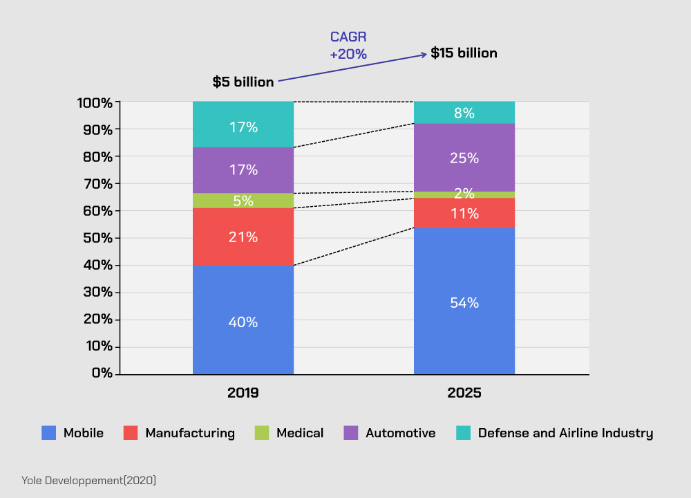
According to last year’s Yole Developpement report* , the 3D image sensor market is expected to achieve an average annual growth rate of 20% from $5 billion in 2019 to $15 billion by 2025. During the same period, the smartphone segment is expected to grow at 26.2% and account for more than half of the 3D image sensor market share by 2025. The automotive segment comes second, as it is expected to record the highest annual growth rate of 27% during this time.
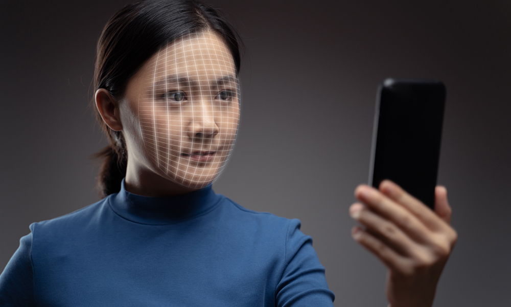
3D image sensors have been used in smartphones since the early 2010s, in features such as AutoFocus* and Proximity Sensing* . In addition, after Apple heavily promoted the Face ID feature—a 3D facial recognition that was first introduced on the iPhone X in 2017—it garnered a lot of attention as a new form factor expected to lead smartphone innovations.
Now, more major smartphone manufacturers, such as Samsung, LG, Huawei, OPPO, and Vivo, are engaged in a tech race to come up with the best 3D image sensors.
How Do 3D Image Sensors Work?
The way 3D image sensors capture images is largely classified into three technologies: Stereo Vision* , Structured Light* , and Time of Flight (ToF). ToF is further divided into two techniques, including Indirect ToF (I-ToF) which measures phase differences and Direct ToF (D-ToF) which measures time differences.
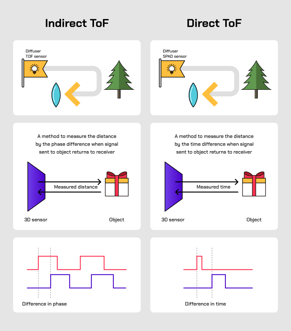
The I-ToF is a method that measures the distance of an object by using lasers modulated at a specific frequency to measure the phase difference using the reflected and bounced signal. Although it is comparatively easier to implement with existing Photodiode (PD) components, it is difficult to measure the distance from objects that are more than a few meters apart because of the low efficiency of photodetectors.
The D-ToF method detects the distance from objects by sending out short pulses of light and then measuring the time it takes for the emitted light to come back. It can measure objects that are ten or a hundred meters away, but a Single-Photon Avalanche Diode (SPAD) would be required.
D-ToF: The Key to Next-Gen 3D Image Sensors
Structured light was used for 3D image sensors in the front camera of Apple’s early iPhone X models, but since then, micro image sensors using I-ToF were developed and are now more widely adopted in smartphones. It is worth noting that Sony, a key player in the image sensor market, secured a high market share with I-ToF image sensors after acquiring Softkinetic Systems S.A. in 2015 to strengthen its image sensor-related offerings.
That said, the importance of D-ToF image sensors will grow even more. Although the number of 3D image sensors in smartphones is expected to increase significantly, they will mostly be installed on the backside of the phone as this would allow for more flexible application than the front. Since 3D image sensors installed in the back should be able to measure distances of more than 5 to 10 meters, it is important for SPAD based D-ToF technology to be researched competitively.
In fact, according to research* by Markets and Markets regarding the ToF image sensor market in 2020, it is estimated that while I-ToF sensors will experience an average annual growth of 11% by 2025, D-ToF sensors will achieve 37.3% average annual growth—more than triple that of I-ToF sensors.
Last year, Apple was the first smartphone provider to add D-ToF sensors in the back—which came equipped on the iPad Pro and iPhone 12 Pro. Apple used SPAD elements and processing technologies from Sony to develop the sensors and referred to them as a LiDAR (Light Detection and Ranging) Scanner to differentiate the technology from existing sensors.
Apple’s LiDAR Scanner can measure up to 5 meters in distance and boasts better performance than I-ToF sensors. When iPhone 12 was launched, Apple emphasized various AR based apps and features by making the most of this technological advantage.
Yole Developpement predicted last year that the 3D image sensor market will grow significantly in 2021 as Apple launched LiDAR Scanner-based smartphones last year. It also predicted that LiDAR sensors for self-driving cars will lead the 3D image sensor market’s growth from 2024* .
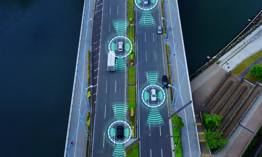
In fact, LiDAR sensors for self-driving cars that deliver precise 3D images with excellent resolution* are in the spotlight as key elements of automated driving. However, current LiDAR sensors are considered inappropriate for mass production as they mostly adopt the mechanical scanning method with motors, making these sensors big and expensive. Thus, D-ToF LiDAR sensors are increasing in demand as they can measure mid to long distances while also being more cost-efficient and compact in size.
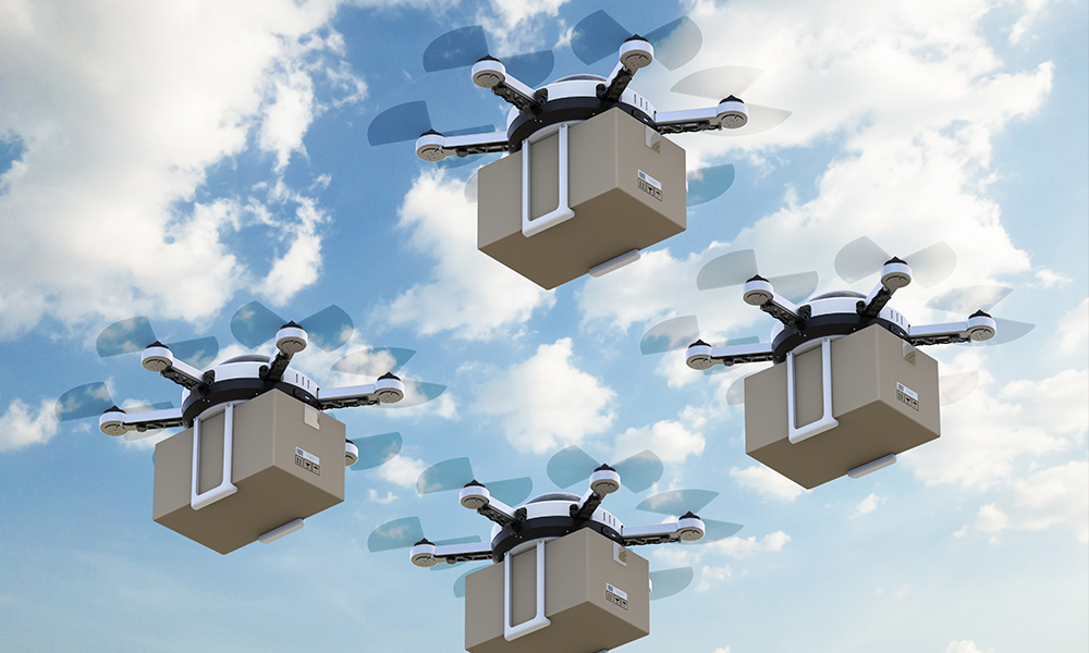
Moreover, D-ToF sensors are expected to play an integral role in the progress of next-generation mobility industries such as robots and drones. A good example is Amazon’s logistics robots and drone delivery service. D-ToF sensors are also considered essential in the factory automation field.
SPAD, An Essential of D-ToF Sensors
Single-Photon Avalanche Diode (SPAD) is a photodetector for next-generation semiconductors that is extremely efficient enough to detect even single photons* due to its very high gain.
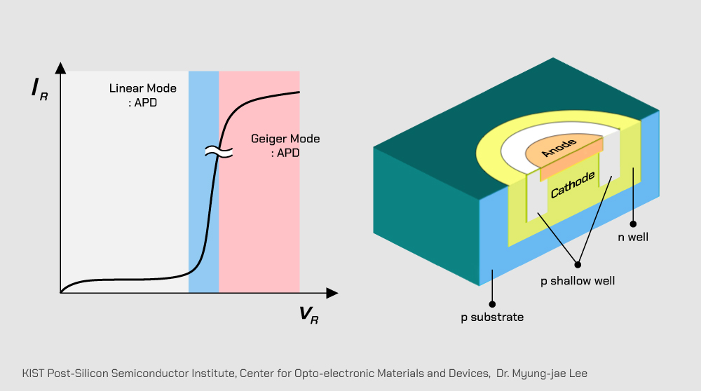
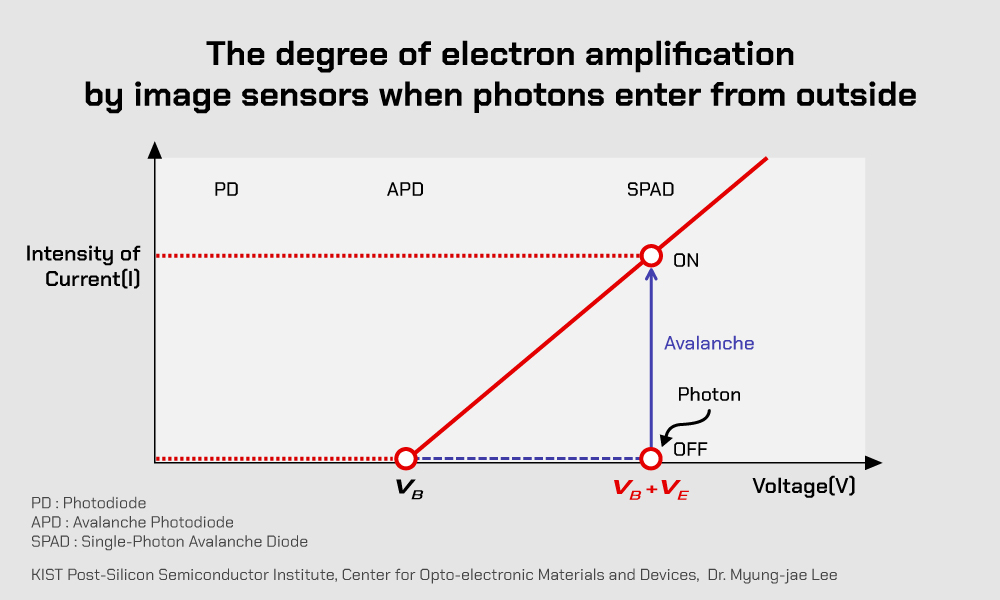
When a higher voltage than the Breakdown Voltage* is applied to SPAD, the impact ionization phenomenon occurs in which a huge electric field accelerates carriers which makes them clash with atoms, increasing the number of free carriers released from the atoms. This phenomenon is called Avalanche Multiplication and results in a large number of free carriers created by photons lit up by image sensors. This means that it can amplify photons and recognize them as a much larger number of photons even though only a small number of them were actually captured, due to dark surroundings or if light was emitted from a far distance.
Also, as SPAD arrays emit digital pulses when photons enter, it is easier to track flight time. Furthermore, it can also capture precise time differences, so it is able to determine accurate depth resolutions* even down to the range of mm and cm.
SPAD-based D-ToF sensors have been successfully verified and researched at Swiss Federal Institute of Technology Lausanne in Switzerland and University of Edinburgh in the UK. STMicroelectronics also adapted the technology to launch proximity sensors which have been applied to a wide range of smartphones.
Just as research and development was carried out using the Backside Illumination (BSI) method to improve performance in image sensors, 3D-stacked BSI SPAD array research has been carried out mainly in the field of SPAD-based D-ToF sensors.12) As mentioned earlier, Apple and Sony have recently collaborated to successfully develop better-performing 3D-stacked BSI SPAD-based D-ToF sensors to mount them on the rear camera of Apple smartphones.
In Korea, researchers from Korea Institute of Science and Technology (KIST) are currently leading the research of essential SPAD for D-ToF sensors to obtain the original technologies and drive the development of the next-generation of 3D stacked BSI D-ToF sensors.
Sony was able to dominate the I-ToF sensor field through its acquisition of Softkinetic Systems S.A., which had the original technologies. Similarly, suppose a key semiconductor company with state-of-the-art technologies and infrastructure, such as SK hynix can actively collaborate with local researchers—we can expect to lead the growing global market of D-ToF and LiDAR sensors.
* ‘CMOS Camera Module Industry for Consumer & Automotive 2020’ by Yole Developpement (2020)
* AutoFocus: A camera technology that automatically focuses on the object
* Proximity Sensing: A feature that detects light waves and recognizes the presence of objects or people. It is used in smartphones to detect user’s face that touches the screen to turn off the screen as to prevent unnecessary touch, and is also used for self-driving and robot technologies to measure the distance between cars or robots and inform the location or access of the objects.
* Stereo Vision: A method measuring the distance to objects with two image sensors and implement 3D images similar to that of human perception of perspective with both eyes. It has a fundamental disadvantage that it’s difficult to miniaturize.
* Structured Light: A method gaining 3D images by shooting certain pattern of light to objects and analyzing the distortion of light pattern returned to image sensor after being reflected from stereoscopic objects, through software. It is difficult to operate accurately under strong light outside, and the software can be costly.
* ‘Time-of-Flight (ToF) Sensor Market – Global Forecast to 2025’ by Markets and Markets(2020)
* ‘CMOS Camera Module Industry for Consumer & Automotive 2020’ by Yole Developpement (2020)
* resolution: An ability to distinguish two objects apart from each other
* Single Photon: A single quantized light particle contrasted with classical electromagnetic wave
* Breakdown Voltage: When the level of reverse voltage is beyond certain limit, it results in Avalanche making huge currents. The voltage in this called Breakdown Voltage.
* depth resolution: An ability to distinguish two objects very slightly apart from each other
* Reference:
https://doi.org/10.1109/IEDM.2016.7838372
https://doi.org/10.1109/IEDM.2017.8268405
https://doi.org/10.1109/ISSCC.2018.8310201
https://doi.org/10.1109/ISSCC.2019.8662355
https://doi.org/10.1109/JSSC.2019.2938412
https://doi.org/10.1109/IEDM13553.2020.9371944
https://doi.org/10.1109/ISSCC42613.2021.9365961
https://doi.org/10.1109/ISSCC42613.2021.9366010