In semiconductor manufacturing, thinfilm deposition refers to the technology of applying a very thin film of 1 µm(micrometer) or less of molecular or atomic materials onto the surface of a wafer. This film allows wafers, which start out in a non-conductive state, to have electrical properties. In other words, it serves as “a blank sheet of paper” to have fine circuit patterns drawn on in the subsequent process. The team in charge of this task at SK hynix is Thinfilm Technology under the Manufacturing & Technology Department.
Our newsroom met with the members of Cheongju NAND M11 CVD and PVD Technology Teams to have a glimpse of their job and the talents they seek to hire.
Uniform Thinfilm Deposition that Meets the Process Conditions
The purpose of thinfilm deposition is to add the electrical properties to the wafers to lay the foundation for the next process. The film is deposited by calculating the thickness of the thinfilm, refractivity, and absorptivity to meet the process conditions. The most important technique is to deposit the thinfilm uniformly throughout the wafer because such uniformity determines the level of precision of the circuit patterns created in the following photo and etching processes.
Among a variety of deposition methods, the most popular ones are Physical Vapor Deposition (PVD) and Chemical Vapor Deposition (CVD).

PVD causes a physical reaction on a metal plate to coat metallic ions on a wafer. As PVD occurs at a low temperature and a high vacuum state, this method has advantages of low contamination from impurities and fast deposition. It is mainly used to deposit a metal layer, which transmits the electric force and signals of the wafer.
A typical PVD method is sputtering. When argon gas is admitted into a vacuum chamber and a high voltage power supply is connected, the gas becomes a plasma. At that point, a negative DC voltage is applied to convert argon atoms into cations. When the cations collide with the metal plate, small amounts of metallic elements are spalled. Sputtering is a method of depositing these metallic elements onto the wafer.
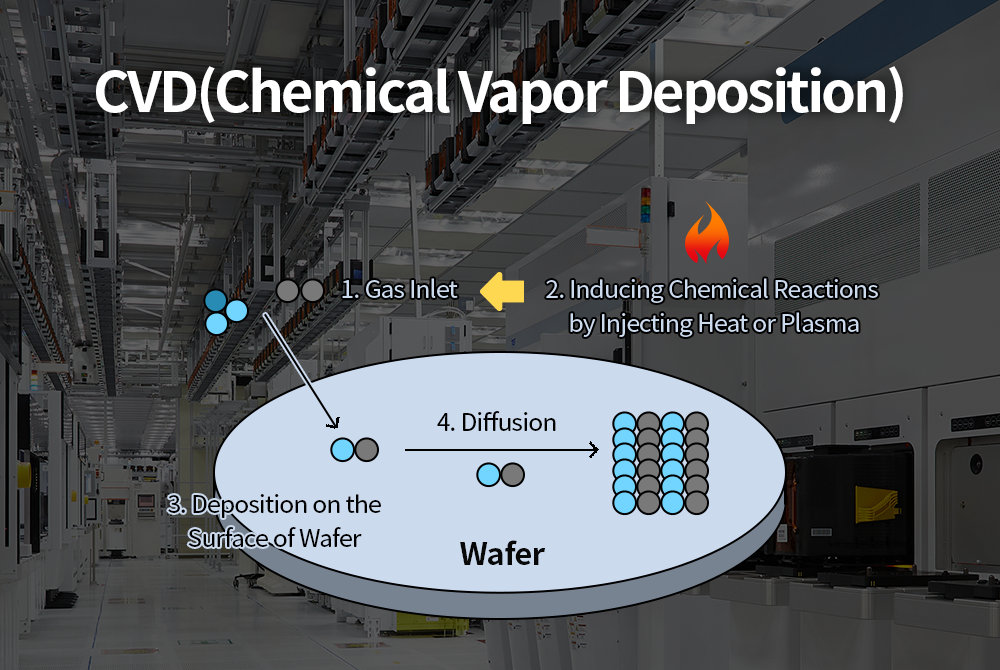
CVD applies heat or plasma to vapor to induce chemical reactions to deposit the output onto the wafer. It has a higher step coverage (the degree of conformity of a film thickness at the bottom/sidewall of a feature to the top of the feature) than PVD. This method is mainly used for the deposition of dielectric layers. Also, it is utilized to deposit Anti-Reflective Coating (ARC), which controls diffuse reflection when drawing patterns in the photo process, or to place a hard mask on the wafer prior to etching to protect the underlying layer.
CVD is classified into four methods based on the operating conditions: Atmospheric Pressure CVD (APCVD), Thermal CVD, Plasma Enhanced CVD (PECVD), and High Density Plasma CVD (HDP-CVD).
APCVD is a CVD method at atmospheric pressure. A high wafer throughput and a simple device structure are big advantages of this process, but it has poor step coverage due to low degree of vacuum.
Thermal CVD uses thermal energy at a high-temperature environment, and the uniformity of the thinfilm deposited by this method is higher than that of APCVD. However, its deposition speed is slow and it poses risk factors due to the high temperature.
PECVD forms thinfilm at a low temperature by reducing the activation energy required for chemical reactions with radicals in plasma. It offers a high throughput and a satisfactory step coverage.
During HDP-CVD process, deposition and etching occur simultaneously performed in the chamber. The deposition is made at a low pressure and high-density plasma state. It is particularly useful for gap-filling the void.
Core Values of Thinfilm: “Technological Innovation for the Best Mass Production Technology”
There are seven teams associated with the thinfilm process: Icheon FAB and Cheongju FAB have both CVD Technology Team and PVD Technology Team, which take charge of deposition under Thinfilm Technology. Technology Innovation Team and Distribution Enhancement Team support the process.
PVD Technology Team performs PVD by using different methods in addition to sputtering, such as reactive ion etching (RIE)1 and the Damascene process2. This is part of their effort to find and implement the optimal deposition for each process. The team has been working on the development of a deposition technology to allow stable formation of a metal line under the cell.
CVD Technology Team is responsible for stable deposition of dielectric layers via HDP-CVD and PECVD methods. It is also in charge of depositing ARC and hard masks, which are essential to increase the efficiency of the subsequent processes. It has recently been focusing on developing a technology that alternately stacks a silicon oxide layer and a silicon nitride layer to make the thinfilm uniform.
Each team is again divided into the Process Part and the Equipment Part according to the nature of the tasks. The Process Part optimizes the process to ensure a stable deposition of thinfilm on the wafer. It also enhances distribution by analyzing the response data and defect data.
The Equipment Part is responsible for equipment maintenance and improving its performance. For instance, it manages the equipment use history, responds to defects in thinfilms, and has the equipment setup or relocated according to the work and production plans.
Technology Innovation Team works on utilizing a variety of data collected from the equipment at each FAB for equipment stabilization while Distribution Enhancement Team is in charge of improving the process distribution at each FAB. These two teams support the teams located in each FAB and contribute to improving the yield.
Although the teams are divided by process, they share the same goal: “achieving technological innovation to secure the best mass production technology.” In doing so, they are constantly communicating with each other and improving the process technology.
Here are some pointers that our engineers want to give you.
Our newsroom met with the junior members of the Thinfilm Technology Department to hear about the competencies and qualities required for their work.

Hyun-do Kim, Technical Leader at Cheongju NAND M11 PVD Technology Team
Q. Please tell us about your job.
I’m a process engineer at Cheongju NAND M11 PVD Technology Team, working on improving the quality of thinfilm. I monitor the entire PVD process of my team to check any issue arising from the in-line (a continuous sequence of operations in the production line). When there is a defect, I analyze the response data and defect data to determine the cause and improve the distribution.
Q. Could you introduce some competencies your job requires?
You have to have a good understanding of PVD technology. It will be helpful to study the properties of semiconductor materials and the principles of physics in the state of vacuum. Also, it is important to make yourself familiar with statistics, especially how to use the tools and interpret the processed data, because we use big data in semiconductor manufacturing.
Q. What challenges have you encountered and how did you overcome?
I find it most challenging when the production quantity and quality issues come in conflict because when we increase production excessively, quality issues arise. To address this challenge, we increase production based on other FABs’ backup evaluations and production increase experiments. We also manage data carefully to prevent any quality issue. Moreover, we are trying to find new data to use for defect analysis.
Q. What are the fascinating aspects of your work?
I love communicating constantly with my team members or other teams to find the cause of the problem when a problem occurs.
Q. What’s the atmosphere of the team like?
We freely express and share our opinions. Whenever we need help, we work together and openly share our thoughts. This process allows us to broaden our perspectives and grow.
Q. What skills are required to complete the work done by your team? What would you say to those who wish to join your team?
A sense of responsibility and attention to details. Due to the nature of our work that deals with thinfilm, there are higher risk of accidents. So, it is important to be detail-oriented and take ownership until the end. Also, those who can communicate well with others are a great fit for our team because we collaborate a lot both within the team and with other teams.

Min-ho Kim, Technical Leader at Cheongju NAND M11 PVD Technology Team
Q. Please tell us about your job.
Part of Cheongju NAND M11 PVD Technology Team, I’m in charge of the equipment that controls titanium (Ti) and titanium nitride (TiN) gases used in the PVD process. My job is project management (PM), which involves equipment operation and work management according to the production volume. When a defect is found in a wafer, I work with process engineers to resolve the problem.
Q. Could you introduce some competencies your job requires?
Semiconductor equipment handles different conditions, such as power, temperature, pressure, and flow, which are applied according to each situation. Therefore, you should be able to take an approach based on extensive knowledge. It is very helpful to build up basic knowledge from major courses in college. Another competency that will help you with this job is competency in data analysis so that you will be able to process the information obtained through parameters monitored in various sensors, such as the equipment’s temperature and pressure, into significant data.
Q. What challenges have you encountered and how did you overcome?
You work with many people as you operate the equipment and solve problems. When a problem occurs in a line, smooth communication between the site and the office is key to taking appropriate measures for the situation. The company offers opportunities for the employees to learn more about semiconductor and important information for different situations, such as SK hynix University (SKHU) classes and Thursday Class organized by Manufacturing & Technology Department every Thursday.
Q. What are the fascinating aspects of your work?
It feels great when I solved a difficult problem by developing a new hypothesis. When an issue arises from wafers during a process, we cannot check the inside of the chamber. Therefore, we have to come up with different hypotheses based on the grounds observed. The process is not easy, but when we find the solution, it becomes the most exciting moment.
Q. What’s the atmosphere of the team like?
PVD Technology Team consists of open-minded people who respect others’ opinions. Such environment has allowed me to develop flexible thinking in doing my job, and it improved my work efficiency as well.
Q. What skills are required to complete the work done by your team? What would you say to those who wish to join your team?
The number one skill, I would say, is flexible thinking. As semiconductor products become more sophisticated, there are times when existing methods are not enough to address an issue. In that case, rigid ways of thinking cannot solve difficult problems; rather, you have to come up with a new hypothesis from the beginning. To future members who will join PVD Technology Team, I recommend that you think of this process as an opportunity to learn something new every day, build your knowledge, and become an expert, rather than as a hard process.

Seung-uk Sim, Technical Leader at Cheongju NAND M11 CVD Technology Team
Q. Please tell us about your job.
I work as a process engineer at Cheongju NAND M11 CVD Technology Team. I manage the process history according to the manufacturing plan and check the interlock3. Another important task is to set up the process in collaboration with related teams when next-generation products are developed or new equipment is transferred.
Q. Could you introduce some competencies your job requires?
The meticulous ability to accurately analyze significant differences in data between equipment is essential. This is because a uniform deposition of thinfilm without physical differences between equipment is indispensable for yield improvement. To this end, you should have the analytical power to quickly share with the team the results collected after deposition.
Q. What challenges have you encountered and how did you overcome?
The biggest challenge for me is when it is hard to find the exact cause of a problem in the process. We work closely with the teams in charge of other processes before and after deposition. We take advantage of the SK hynix Big Data Analysis System to identify the problem and implement the interlock to prevent the same issue from reoccurring.
Q. What are the fascinating aspects of your work?
I love about being able to work with others and achieve something that cannot be done by myself. Due to the nature of my job, I get to collaborate with related teams using output values. Whenever that happens, I get to learn about other processes and solve problems, so it’s like having my cake and eating it, too.
Q. What’s the atmosphere of the team like?
The image of the semiconductor manufacturing industry seen from the outside is “rigid”. However, CVD Technology Team is a flat organization that welcomes fresh ideas from new members.
Q. What skills are required to complete the work done by your team? What would you say to those who wish to join your team?
As long as you are passionate about solving problems and not afraid of challenges, you can overcome any difficulties after joining the company. In particular, Thinfilm Technology Department offers a well-structured training program for the newcomers, so you will be able to see yourself grow in the team.

Tae-wook Cho, Technical Leader at Cheongju NAND M11 CVD Technology Team
Q. Please tell us about your job.
I work at the Equipment Part at Cheongju NAND M11 CVD Technology Team. I establish PM plans for the stable operation of mass production equipment, and I also set up new equipment or transfer surplus equipment. I am also responsible for reviewing issues arising from the equipment and resolving the problems in collaboration with related teams.
Q. Could you introduce some competencies your job requires?
Being detail-oriented is important to work in the Equipment Part. Some problems occur in the equipment because a very minor detail has not been properly addressed. It is necessary to check the equipment and its operation meticulously to prevent this from happening.
Q. What challenges have you encountered and how did you overcome?
Not only does it take a lot of time and manpower to solve a chronic problem of a piece of equipment, but it is also difficult to define the cause even after solving the problem. That is why I manage the equipment history and data constantly and prioritize different problem-solving approaches. I also go into the production line to see and touch the equipment myself to improve it.
Q. What are the fascinating aspects of your work?
I once worked on setting up new equipment in a FAB. I basically had to prepare every single piece of equipment for the FAB and it felt like I was making something out of nothing. I felt proud to see the equipment contributing to production.
Q. What’s the atmosphere of the team like?
Since the company introduced a flextime system, individuals have been given more autonomy at work. We can work flexibly under certain standards, which has helped us improve our work-life balance.
Q. What skills are required to complete the work done by your team? What would you say to those who wish to join your team?
I would suggest they show that they are hard-working people who are also willing to learn. All the efforts and experiences you have made to join our company will pay off and form the basis of your work at SK hynix. Be confident and believe in yourself.
1Reactive ion etching (RIE): It is part of the metallization process, which “creates a path for electricity.” In this method, aluminum (AI) films are first deposited, followed by the photo process and some AI etching, Then, non-metallic films of silicon dioxide (SiO2) are deposited.
2Damascene: It is part of the metallization process. Non-metallic films of silicon dioxide (SiO2) are deposited, followed by the photo and etching processes to create patterns. Then, metal films are deposited inside, followed by the chemical mechanical polish (CMP) process, thereby creating independent metal lines.
3Interlock: A system that shuts down the equipment when any of the optimized process criteria is not met. The shutdown continues until all the criteria are met. Its purpose is to minimize product defects.