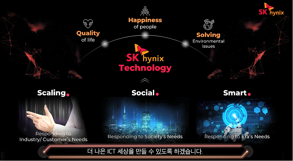
– To respond to industrial changes with the scaling, social, and smart values and pursue a better future through boundless cooperation
– Jin Kook Kim, Head of R&D, and Seon Yong Cha, Head of DRAM Development also explain Financial Story at major forums
Top executives of SK hynix including CEO Seok-hee Lee set out to actively promote the company’s Financial Story1.
On March 22 (Korea Standard Time), CEO Seok-hee Lee gave a keynote speech to the Institute of Electrical and Electronics Engineers (IEEE) International Reliability Physics Symposium (IRPS) and shared with the industry experts the Financial Story pursued by SK hynix. For 59 years, IEEE IRPS (https://irps.org/) has been the prestigious premiere conference for engineers and scientists in the microelectronics field such as semiconductors, communications and systems from the United States, Europe, Asia, and all other parts of the world to present new and original work in the areas of reliability.
CEO Seok-hee Lee, who has received the Distinctive Exemplary Industry Leader Award for 2020 from the IEEE Consumer Technology Society (CTSoc) in January, gave a keynote speech on the theme of “Memory’s Journey towards the Future Information & Communications Technology World”. In this keynote speech delivered in a video, CEO Lee presented prospects on the future of semiconductors amid the upcoming changes in the ICT industry. He also announced SK hynix’s strong will to develop technologies considering the scaling, social, and smart values to pursue both economic value (EV) and social value (SV) at the same time for a better ICT world.
“Semiconductor Memory is the Center of the Future ICT World and We Will Make a Better World through Advanced Technology”
CEO Seok-hee Lee began his keynote speech by introducing the accelerated digital transformation of the 4th Industrial Revolution due to COVID-19. As non-face-to-face activities including ICT-based remote education and telecommuting have become a large part of everyday life, the use of data has rapidly increased recently.2 In particular, with the advances in new technologies such as 5G, autonomous vehicles, and artificial intelligence (AI), the amount of data generated and consumed in real-time is showing an explosive increase. Accordingly, the global data center market continues to grow and the demand for DRAM and NAND, which are essential for this growth, is expected to increase significantly.3
Semiconductor Memories, which used to be simply used for servers, PCs, and mobile devices, are now expanding and diversifying in terms of their functions amid various technological innovations. CEO Lee emphasized that, for this reason, semiconductor memories will play a role beyond storing and processing information in the future, as the core of the future ICT world.
Also, CEO Lee explained that achieving a high level of reliability is important to realize technological innovation suitable for the smart ICT environment in the “digital transformation of the 4th industrial revolution”, while the existing semiconductor memory industry has been mainly focusing on implementing “high density, high speed, and low power” to respond to various applications and customer needs so far.
In addition, CEO Lee said that as now is the time for companies to take the lead in resolving pain points of the stakeholders – in other words, various social problems such as energy shortage and climate change – the semiconductor memory industry is facing the needs of times to create a better future through technology in addition to the traditional values that have been provided until now.


Furthermore, SK hynix emphasized its will to create a better world through advanced technology by pursuing the Financial Story and encouraged all members of the semiconductor ecosystem to interest, support, and participate.
“In the era of fierce competition for miniaturization, the matters of technology completion and productivity were dealt with through vertical relations with suppliers. Now, however, is the time when various partners building the semiconductor industry ecosystem must form a cooperative partnership. Only by establishing a strategic partnership for Open Innovation4 based on collaboration and sharing with customers, suppliers, academia and government, we can shape a new era, which pursues both economic and social value.
SK hynix will take the initiative in enhancing the quality of our lives, solving environmental issues, and pursuing the happiness of our employees and stakeholders. We will incorporate scaling, social and smart value to the technology development to achieve the ultimate goal of making a better ICT world. We ask for your interest, support, and hopefully, your participation in pursuing social values and actively responding to the needs of the era with technology.”
“Realizing Scaling, Social, and Smart Values is the Prerequisite for the Semiconductor Technology Development”
CEO Lee shared various management strategies that SK hynix is preparing to create a better future through technology. In particular, he highlighted that the three values of scaling value, social value, and smart value will lead the development of semiconductor technology in the era of digital transformation. He also announced plans to enhance reliability, as well as various efforts that SK hynix is making in each field.

“Scaling Value” means satisfying the needs of industries and customers by solving the problems of innovation and reliability in materials and structures for the evolution of DRAM and NAND technologies.
CEO Lee introduced some key tasks for DRAM and NAND respectively to achieve this goal. As the key tasks, “overcoming the limitations of patterning in lithography, maintaining the capacitance of the cell capacitor, and lowering the resistance of the metal for interconnect” were mentioned for DRAM and “securing high aspect ratio contact (HARC) etching technology, securing cell dielectric characteristics, and solving film stress issues” for NAND.
In the DRAM field, SK hynix has introduced extreme ultraviolet (EUV) lithography equipment to overcome the limitation of patterning and is making great efforts to improve productivity, such as developing materials and photoresists for stable EUV patterning and defect management. Also, in order to maintain cell capacitance (Cs), the company is trying to refine the dielectric thickness, develop new materials with high dielectric constant, and innovate the cell structure. In regards to the low resistance metal for interconnect, the company is seeking next-generation electrode and insulating materials and introducing new processes. For applications that require high reliability such as automotive semiconductors, SK hynix is applying the optimized process technology to increase the tolerance to soft errors5 and overcome this challenge.
In the NAND field, SK hynix is focusing on securing etching technology to implement high aspect ratio (A/R) to realize the high density technology required by the industry. Also, the company introduced the atomic layer deposition (ALD)6 technology to further improve the cell property of efficiently storing electric charges and exporting them when needed, while developing technology to maintain uniform electric charges over a certain amount through the innovation of dielectric materials. In addition to this, to solve film stress issues7, the mechanical stress levels of films is controlled and the cell oxide-nitride (ON)8 material is being optimized. To deal with the interference phenomenon between cells and charge loss that occur when more cells are stacked at a limited height, SK hynix developed the isolated-charge trap nitride (isolated-CTN)9 structure to enhance reliability.
CEO Lee said, “We are improving materials and design structures for technical evolution in each field of DRAM and NAND, and solving the reliability problems step by step. If the platform is innovated successfully based on this, it is possible to achieve the DRAM process below 10 nanometers (nm) and stack over 600 layers of NAND in the future.”
“Social value” means using technology to contribute to solving various social problems such as energy, disease, and environmental problems, as well as creating economic value, and fulfilling social responsibilities through this. It is expected that environmental problems and energy shortage problems, especially climate change, will become more serious in the future. For this reason, countries in Europe, the United States, China, and many other countries have declared the goal to achieve net-zero10 to reduce greenhouse gas emissions, which are the main causes of global warming.
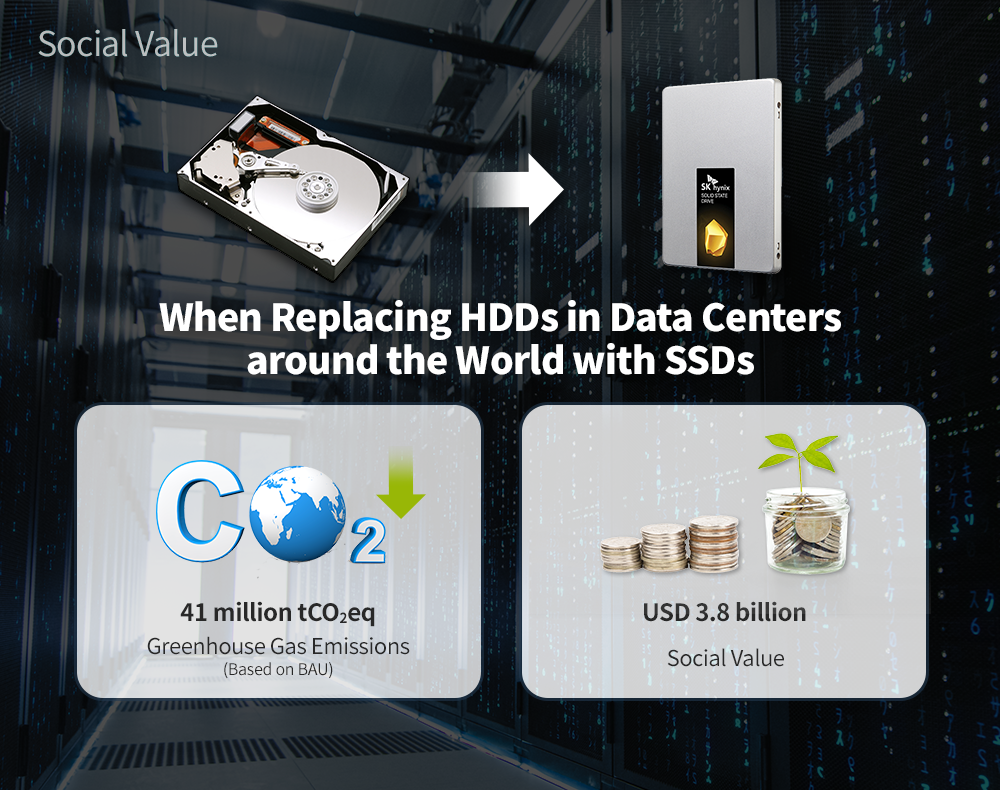
It is indeed difficult to improve the increasingly deteriorating global environment with the current hard disk drive (HDD)-based data storage system and power generation technologies. Accordingly, CEO Lee emphasized that the semiconductor memory industry should accelerate technological innovation to focus on solving these problems.
If HDDs in data centers around the world are replaced with low-power PLC/QLC-based solid-state drives (SSDs), greenhouse gas emissions can be reduced by approximately 41 million tons, based on business as usual (BAU)11 estimates and this can create social values worth more than USD 3.8 billion.
With the social demand to compute explosively increasing data at a high speed and low power, computing and memory systems are changing as well. Accordingly, CEO Lee explained that the memory is developing into a heterogeneous memory technology that is more specialized in a single characteristic such as speed or low power. Some of the representative memory solutions are High-Bandwidth Memory (HBM)12 for high-speed processing, Ultra-low Power Memory (ULM)13 that consumes much less power, and Compute Express Link (CXL)14, interface solution memory that is newly emerging.
CEO Lee emphasized that social responsibility through semiconductor technology does not end here. He said, “If we were to follow the current path based on the current solution alone, soon, we will reach the first critical point. So, to delay reaching the critical point, convergence solutions suitable for each era should be delivered not only to greatly reduce the energy consumption in computing but also to improve the computing performance.”

“Smart Value” means preparing for a new, approaching era, by completing an intelligent memory solution suitable for the post-digital-transformation era. In the future, all devices will be integrated based on AI technology and smart ICT technology will be used in everything surrounding us. This means a hyper-connected era where all societies are connected faster with much less power through the convergence of semiconductors, AI, and telecommunication technologies.
To prepare for this future, CEO Lee introduced the “disruptive innovation” carried out at SK hynix at the moment and presented the direction of the evolution of memory semiconductors in the post Von Neumann era.
CEO Lee predicted that semiconductor memories will develop toward a convergence of memory and logic to overcome the performance limitations, in the era of New ICT where all devices are integrated based on AI technology. This means that some of the computing functions of the central processing unit (CPU) are given to the DRAM functions. As the speed was increased in HBM by increasing the number of channels between the CPU and the memory, the speed will increase further in PNM (Processing Near Memory), where both the CPU and the memory exist within a single module. The speed will further increase in PIM (Processing In Memory), where the CPU and the memory exists within a single package. Ultimately, speed will increase further in CIM (Computing in Memory), where the CPU and the memory is integrated within in a single die, to deliver high performance computing system.
In addition, CEO Lee predicted that the memory technology of the post Von Neumann computing era will evolve to neuromorphic semiconductors15, and storage technology into the same form as the DNA semiconductors16. He emphasized that ultra-high-speed computation and storage will become possible even with a small amount of energy human brain uses. Also, he stressed that it will become possible to enable a true smart world, where the same large amount of data can be stored and processed at low power in a small room without having to maintain a hundred thousand square meters of data centers.
CEO Lee emphasized SK hynix’s will for the future by saying, “SK hynix is preparing for the future by taking the evolutionary path and the revolutionary path to respond to changes in semiconductor memories. We will continue to incorporate the value of scaling in the conventional memory, to include social value in the next generation memory and intelligent memory, and to contain the value of smart in the post von-Neumann era.”
Jin Kook Kim, Head of R&D, and Seon Yong Cha, Head of DRAM Development Also Spread the Financial Story at Semiconductor Forums Earlier This Year
Earlier this year, Jin Kook Kim, Head of R&D, and Seon Yong Cha, Head of DRAM Development also participated in spreading the Financial Story through keynote speeches at a major semiconductor academic conference.

Presentation by Jin Kook Kim,
Head of R&D, at the Korean Conference on Semiconductors
Presentation by Jin Kook Kim,
Head of R&D, at the Korean Conference on Semiconductors

Presentation by Jin Kook Kim, Head of R&D,
at the Korean Conference on Semiconductors
At the 28th Korean Conference on Semiconductors held on January 26, SK hynix’s R&D Head Jin Kook Kim gave a keynote lecture on the theme of “Future of Semiconductor Technology” and explained SK hynix’s Financial Story, as well as the strategies for the semiconductor memory business implemented by SK hynix.
“The semiconductor industry has had a traditional mission of overcoming the limitations of miniaturization and providing value for customer needs. In addition to this, I believe that the industry now faces a new mission of responding to social responsibilities including energy and environmental issues and meeting the spirit of times to create a better world through technology.”
As a technological strategy to overcome the limitations of the explosive increase in data, changes in computing and memory systems are underway. In the case of CPU, it is developing in the form of multi-core, many-core, and heterogeneous computing, which is a heterogeneous computing technology such as mixing CPU and GPU. Likewise, in the case of memory, a heterogeneous memory technology specialized for density or speed is required, instead of the previous direction for simultaneously increasing capacity and speed.
Kim said that in order to respond to these changes, SK hynix is preparing high-speed processing, low-power, and heterogeneous computing interconnect technology memories, respectively.
Also, Kim said that memory will play a key role in heterogeneous packaging or integration that combines micro-electro-mechanical systems (MEMS), radio frequency identification (RFID), sensors, and even biochips.
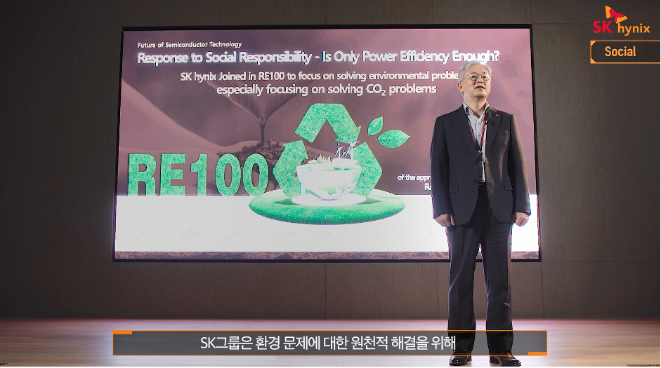
Kim said, “SK hynix’s social responsibility through semiconductor technology does not stop here, but we are also making efforts for the environment and energy. SK Group has joined RE10017 for the fundamental resolution to environmental issues and plans to convert 100% of the electricity consumed to renewable energy by 2050.”


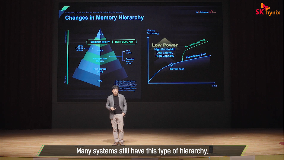
On February 3, Seon Yong Cha, SK hynix’s Head of DRAM Development gave a keynote speech on the theme of “Economic, Social, and Environmental Sustainability in Memory” at SEMICON KOREA 2021. During his speech, he highlighted the necessity of environmental preservation in the semiconductor industry and introduced SK hynix’s efforts to achieve this.
“Transmitting data requires a huge amount of energy. As the amount of data used increases, greenhouse gas emissions also increase as well as power consumption. As a company that develops semiconductor memories, it is essential to consider the environmental impact. Furthermore, the semiconductor industry should also further strengthen its social responsibility for environmental preservation by reducing energy consumed in the future.”
SK hynix has joined the RE100 with SK Group’s subsidiary companies for the first time in Korea and declared that it will replace all the power required in the semiconductor manufacturing process with renewable energy by 2050. Along with these efforts, SK hynix is developing semiconductor technologies including HBM, ULM, and accelerator-in-memory (AiM)18.
All of these HBM, ULM, and AiM products have a great possibility of improvement in terms of performance and power depending on how close they are to the system on chip (SoC)19 or how they converge. For this reason, SK hynix plans to expand the portfolio for this and is collaborating in different ways to develop various solution products in addition to the existing standard products.
DRAM Development Head Cha said, “To strengthen further the social responsibility for environmental preservation through energy saving, cooperation across different fields including academia, semiconductor, equipment, SoC, memory, and software is necessary, and SK hynix will actively cooperate for this.”
※ IEEE IRPS2021, https://irps.org
1Financial Story: SK Group’s new management strategy to increase the total value that includes corporate value by presenting the growth strategy and future vision of each subsidiary company of SK to various stakeholders such as customers, investors, and the market, generating trust and sympathy. SK hynix has established and initiated in earnest its Financial Story to contribute to humanity and society by strengthening ESG while pursuing continuous business growth through DRAM and NAND as two main pillars.
2According to the “2020 4th Industrial Revolution Index” announced by the Ministry of Science and ICT of Korea in September 2020, the number of IoT device service subscriptions increased by 21.6%, from 21.44 million in June 2019 to 26.07 million, in one year. The 5G data usage increased by 2,328% in one year, from 5,938 terabytes (TB) in April 2019 to 144,192 TB.
3The industry predicts that the 5G technology, which is 10 to 100 times faster than 4G, can provide an environment where more data can be transmitted accurately and quickly. Also, it is predicted that more than 4 TB of data will be generated a day per car to implement an autonomous driving environment. Data centers around the world are expected to grow at 15% Compound Annual Growth Rate (CAGR) from 2015 to 2025, reaching the double level in 2025 compared to the current level. In general, one data center requires 20 million gigabytes (GB) for the DRAM capacity and 750 million GB for NAND capacity.
4Open Innovation: It refers to a paradigm that assumes that firms can and should use external ideas and technology required and share the internal resources outside the firm to create a new product or a service. The term is widely used in various fields after Professor Henry Chesbrough of UC Berkeley proposed the concept in his 2003 publication.
5Soft error: An error in which the data stored in the semiconductor memory changes due to energy ion collision. It is not physical damage, and the semiconductor memory operates normally when data is re-written or the device is reset. Alpha particles emitted from radioactive impurities or ionized secondary particles by external high-energy neutron reactions are the main cause.
6Atomic layer deposition (ALD): Nano-scale film deposition technology that uses the phenomenon where monoatomic layers are chemically attached during the semiconductor manufacturing process; through this technology, foreign materials are deposited homogenously and rapidly. By alternately absorbing and displacing molecules on a wafer surface, it is possible to realize atomic-layer thick ultra-fine layer-by-layer deposition and stack oxide and metal films as thin as possible.
7Film stress: A phenomenon where a wafer is bent or curled due to pressure, force, etc., applied to a specific area on the wafer surface
8Cell oxide-nitride: A film material that prevents electrons stored in floating gates from escaping or tunneled electrons from crossing floating gates
9Charge trap nitride (CTN): A layer acting as a floating gate in the 2D NAND structure; to solve the problem of the interference between cells when implementing 3D NAND, SK hynix changed the floating gate method of storing electric charges in conductors to the charge trap method of storing them in insulators.
10Net-zero: Reducing greenhouse gas emissions generated by human activities as much as possible and absorbing and removing remaining greenhouse gases so that actual emissions become zero.
11Business as usual (BAU): A total amount of greenhouse gas expected if no artificial measures are taken to reduce greenhouse gas emissions
12High-Bandwidth Memory (HBM): A high bandwidth product that can transmit a large amount of data at once; it can improve energy efficiency by about 40% in terms of power consumption.
13Ultra-low Power Memory (ULM): A product designed to replace static random-access memory (SRAM); it can increase density by 100 to 1,000 times compared to SRAM and can improve energy efficiency by four to five times compared to HBM.
14Compute Express Link (CXL) Memory: Apart from the existing memory interface, DDRx, it is a heterogeneous computing memory interface called ‘Compute Express Link’. Bandwidth & Capacity expansion memory, Persistent memory and Pooled memory can be implemented. Major Datacenter industry Eco. Players are participating in the CXL consortium.
15Neuromorphic means the form (morphic) of a neuron and a neuromorphic semiconductor imitates the structure of a cranial nerve.
16DNA semiconductor: A semiconductor that artificially implements the principle of data storage of DNA that can store about 1 billion GB of data per 1 ㎟ in theory; DNA semiconductors store data by converting the conventional data based on the binary method consisting of 0s and 1s into four base sequences of DNA: adenine, guanine, cytosine, and thymine.
17Renewable Energy 100 (RE100): A declaration to procure 100% of the power consumed with renewable energy. Renewable energy refers to wind power, geothermal heat, fuel cells, hydrogen energy, etc.; through this, companies can operate factories and produce products in a more eco-friendly way by reducing the carbon from petroleum, coal, etc., emitted to generate electricity.
18Accelerator-in-memory (AiM): A type of PIM that adopts the offloading concept that adds the roles of the existing CPU, such as computing function; into the memory, it is possible to improve the performance bottleneck caused by the memory in systems.
19System on chip (SoC): A single chip that integrates the core parts used in information and communication devices into a single semiconductor, enabling the operation functions previously performed by multiple chips, such as data storage and converting the analog and digital signal, being realized on a single chip.