Hit enter to search or ESC to close
ENG
English
Chinese(中文)
Korean(한국어)
ENG
中文
KOR
Press Release
Business
Multimedia
Technology
Culture & People
ESG
Opinion
Fact Sheet
Earnings
아이콘
Sustainability Report
아이콘
PRESS CENTER
Press Release
Business
Multimedia
INSIGHT
Technology
Culture & People
ESG
Opinion
CORPORATE
Fact Sheet
Earnings
아이콘
Sustainability Report
아이콘
PRESS CENTER
INSIGHT
CORPORATE
Search
PRESS CENTER
PRESS CENTER
Press Release
Media Gallery
Event
INSIGHT
CORPORATE
MULTIMEDIA
INSIGHT
CORPORATE
MULTIMEDIA
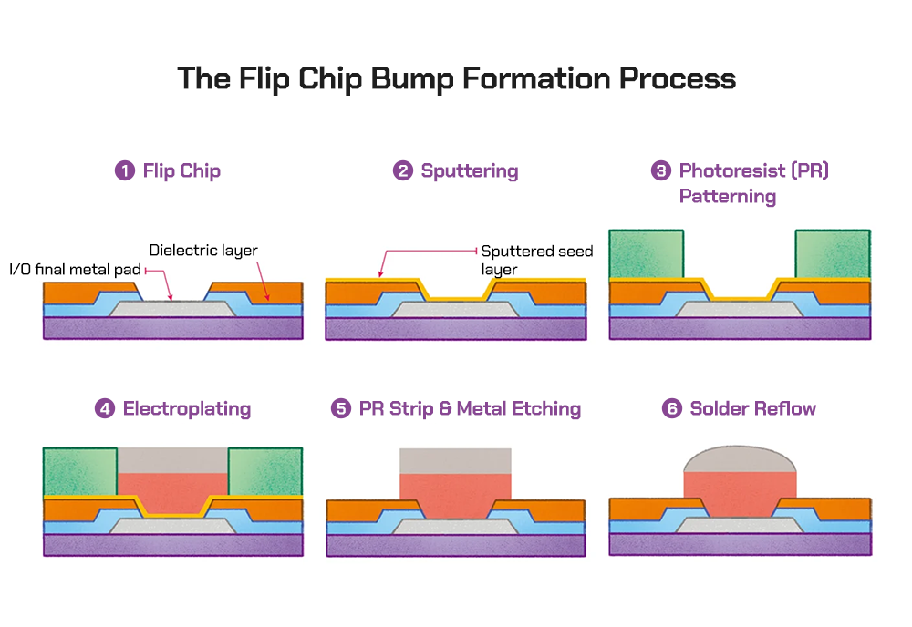
SK hynix_Semiconductor Back-End Episode 8_Image 03
Leave a Reply
Cancel Reply
Name
*
Email
*
Website
Save my name, email, and website in this browser for the next time I comment.
PRESS CENTER
PRESS CENTER
Press Release
Media Gallery
Event
INSIGHT
CORPORATE
MULTIMEDIA
INSIGHT
CORPORATE
MULTIMEDIA