The core of semiconductor memory technology and business is the ‘expansion of density.’ This means that the semiconductor includes a lot of bits, the unit that distributes or contains information. There are various requirements on the demand side of semiconductor memories, including speed and reliability, but the demand for storage space is the highest of all.
You would think that if density is high, storage capacity will be enhanced, and therefore, the semiconductor to be more expensive. But the price of a semiconductor memory chip is not proportional to its density. In fact, it is unrelated to density, or fluctuates inversely to density in the range of one US dollar to eight US dollars. Around 40 leading companies around the world that failed to adapt fell behind. And only three to four companies that manufactures DRAM and NAND, respectively, survived, enjoying the global market for the past decade.
Then, what correlation is there between memory density and the cost of semiconductor products? And what impact does these factors have on the memory semiconductor market?
1. The law of increasing semiconductor memory density, about 1,000 times (2* ) a decade
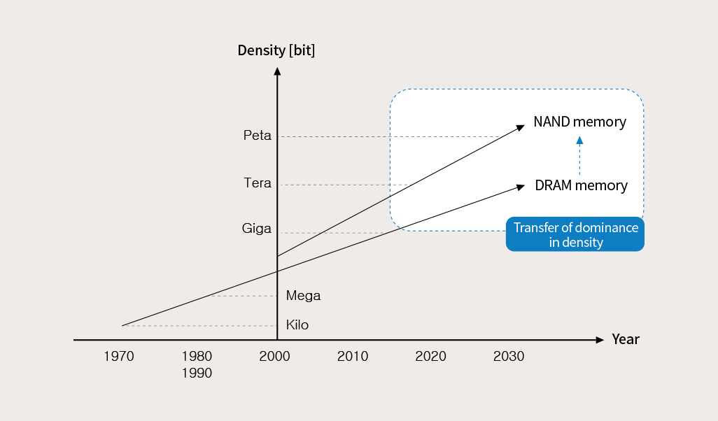
▲ Figure 1. Yearly comparison of density increase trends between DRAM and NAND
The density of semiconductor memories began with 1Kbit DRAM in the 1970s and showed a trend of increasing by about 1,000 times (2* ) in every 10 years. The 1980s was the age of the megabit and the 1990s and the 2000s were a time when the megabit increased to the gigabit.
However, the true winner of actual density in memory was NAND, which appeared in early 2000. At first, in the initial stages of NAND, SLC products of less than 1Gbit in capacity, or 128Mbit (Mega: 2* ) and 256Mbit, appeared in the market. After a decade, MLC products of about 1,000 times the capacity, or 64Gbit (Giga: 2* ) and 128Gbit, became the mainstream. Recently, in the early 2020s, TLC products of terabit (2* ), which is 1,000 times the Gbit, started to become the mainstream product.
This shows a trend of NAND density increasing by around 1,000 times over 10 to 15 years. With this trend, the era of the petabit (2* ) (QLC-NAND), which is 1,000 times the terabit, will come in the early 2030s. One book takes up less than 10Mbit and a movie at around 20Gbit, meaning that 1Tbit will allow you to save more than 100,000 books you will read in a lifetime or dozens of movies.
For DRAM, 64Gbit to 128Gbit products (DDR5) have been released recently, maintaining a density of 1/100 times the density of NAND in 2020. It is expected that this gap will widen over time, showing a 1,000-fold gap in 2030 and more than a 10,000-fold gap in 2040.
2. Maximizing density and minimizing chip surface area → Leading prices
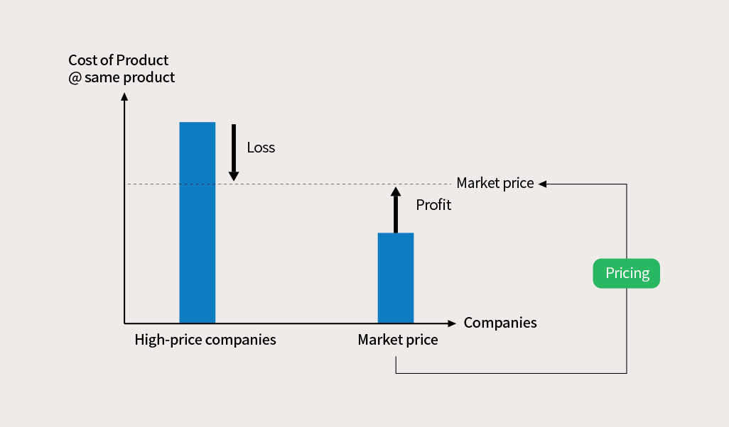
▲ Figure 2. Pricing structure of semiconductors
Suppliers focus on increasing density per chip or the number of chips in a wafer to the maximum to lower the sales price or unit cost of semiconductors. The purpose of increasing density per chip is not only because of the demand for storing as much data as possible in the chip, but also because customers continuously seek a continuous cost down in semiconductors. On the other hand, the reason for increasing the number of chips in a wafer, or Net Die, is because the supplier wishes to achieve cost saving regardless of the demand of the market. In other words, higher specification in density is in line with the common interest of both suppliers and demanders, while the increase in the number of chips or net die purely contributes to the supplier’s profits.
Here, the supplier increases density per chip and net die per wafer to satisfy both needs (high density, cost saving) at the same time, while additionally lowers its profits. This is due to the semiconductor ‘chicken game,’ trying to overwhelm competitors in the market by adopting a strategy of lowering profitability, but increasing market share instead. In this case, the supplier must create an environment where it gains profit, but its competitors lose. This is only possible when there is a significant gap between the supplier’s cost and its competitors’ cost.
A supplier that wins in the cost competition can gain a dominant position in pricing and therefore, suppliers mobilize all capabilities, including technology and sales condition, and pursue a low-cost policy to increase global market share. If this continues, competitors will fail to improve profit structure and inevitably be thrown out of the market. For example, the former global DRAM semiconductor company Elpida Memory and German company Infineon lost in the chicken game and sold its DRAM business or withdrew from the market despite many efforts made at the national level to revive the companies.
2-1. Maximizing density → Forming low cost per production of bit
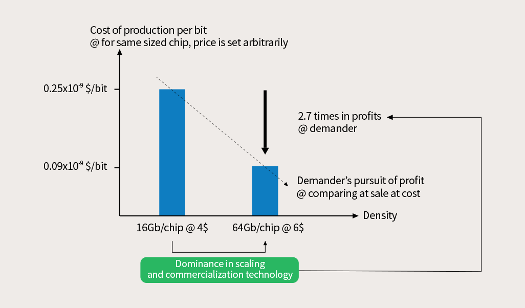
▲ Figure 3. Lowering production cost of bit by increasing chip density @ chip price set arbitrarily
Typically, increasing density is about planning a new product, designing based on device technology, and completing its features and reliability accordingly. To increase density, you need to either increase the number of cells physically even if it leads to a slightly larger chip size or increase the number of bits electronically. In semiconductors, physical cells refer to transistors (TR) and therefore, one must make TR smaller or minimize the width of circuit lines that connect TRs. These are some examples of conventional scaling down in semiconductor memories and can be applied to all memories, including DRAM and NAND.
Manufacturing by only increasing the number of bits is a method that differentiates based on the level of storage capacity of electrons within the cells of a certain size. This is not a physical method and therefore has no relevance with the size of TR or circuit linewidth. Increasing number of bits within the physical cell is only an option applicable to NAND. Currently, major NAND products can store three bits of information per cell (triple-level-cell, TLC). DRAM, which stores 1 bit per cell, must lower the cost per bit through physical methods, while 3 bits-per-cell NAND has the upper hand being able to use both physical and electronical methods. Therefore, the leading role in the development of memory density has transferred from DRAM to NAND. For various reasons, DRAM costs more than 10 times NAND in terms of cost per bit.
When the density of a product is increased, the price of the product goes up as well. The incremental price increase, however, is smaller than the incremental density increase. So, even if the price goes up by 1.5 times, the density mostly increases by 4 times (2 to 4 times), meaning that demanders enjoy a gain of more than 2.5-fold. In other words, even if a new semiconductor product is offered at a high price, the density increases more than the incremental price increase, making it beneficial to demanders, while also creating a favorable structure for suppliers by forming a lower price per bit. However, in reality, density increase leads to larger chip size along with other variables. And the launch price, unlike during the planning phase, may vary according to market variables such as the timing of the release.
2-2. Minimizing chip size → Forming low cost per production of chip
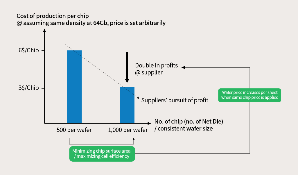
▲ Figure 4. Lowering cost per chip by increasing number of chips per wafer
@ number of chips and price set arbitrarily
Increasing the number of chips per wafer requires minimizing the surface area of chips physically. This requires reducing the width of circuit lines or maximizing cell efficiency to reduce chip size. But narrowing the linewidth of circuits makes the reliability and function of device (TR) vulnerable. Therefore, the design rule is to find the optimal design requirement to increase the number of chips because there is a limit to making cell size smaller.
The design rule, in the narrow sense, refers to the layout of the optimal conditions for conductor linewidth and the physical space between conductor lines, while ensuring the electrical characteristics of the design. However, in the broader sense, design rule refers to setting up the optimal conditions for various factors, including process state, physical form of package, and permitted electrical condition. Maximizing number of chips per wafer can increase the price of wafer per sheet which ultimately helps suppliers reduce cost per chip.
3. The rise and fall of IDM companies
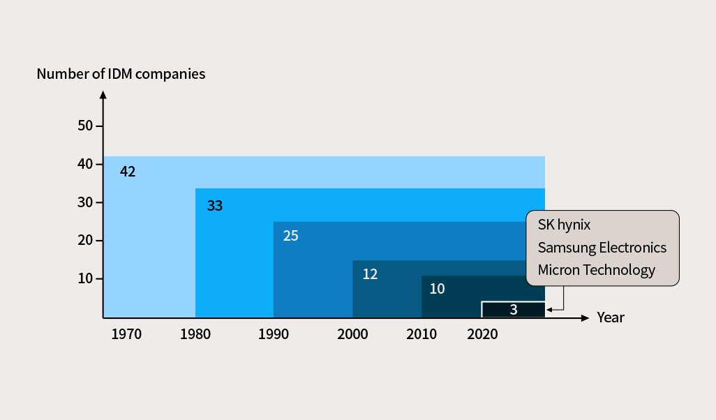
▲ Figure 5. Yearly changes in the number of global DRAM IDM companies
@ excluding companies with less than 3% market share in global DRAM market
Starting with Intel in 1970, the semiconductor memory business was considered as a profitable business. About 20 American electronic companies entered the business, making it a US-led industry. In the 1980s, around 10 global electronic companies in Japan led by Hitachi also entered the market, creating a booming semiconductor industry. Since then, the semiconductor craze spread to Korea, establishing a 3-pillar structure among Samsung Electronics, SK hynix (former Hyundai Electronics), and LG Semiconductor. Semiconductor also became a good business to almost 10 ITC companies in Europe, including SGS-Thomson Microelectronics. As a result, about 40 companies entered the market from the 1970s to 1990s, but around 10 companies disappeared every decade due to cost-saving war. After two fierce chicken games in the industry, companies that were once outstanding with great technological prowess disappeared from the market. And currently, three DRAM IDM companies (Samsung Electronics, SK hynix, and Micron) and four NAND IDM companies (Samsung Electronics, SK hynix, Kioxia (former Toshiba), and Micron) are solidifying their status and position.
There are several options other than what have been introduced today in increasing density and lowering cost. Measures, including evolving from 2D to 3D, applying EUV and new processing methods, increasing number of bits per cell (NAND), TSV (DRAM) and structural improvements like 4D, are made in multifaceted approach. It is expected that PCRAM, MRAM, ReRAM and other types of new products based on the concept of NAND will contribute as next-generation memories. The strategy of balancing product pricing through cost saving can appear anytime in the demander-favorable market, while suppliers can also take the challenging environment as an opportunity to surpass competitors significantly.