

All three primary colors of light – red, green and blue – are required for LED using semiconductors to display full color and realize white light; however, unlike red and green LEDs developed in the 1950s and 1960s, blue LEDs remained extremely difficult to develop until the 1990s despite numerous efforts worldwide. This is because the quality issue of gallium nitride (GaN), which is critical for realizing blue LED, had not been solved.
The industry and academia concentrated on the development of blue LEDs because white LEDs made of red, green and blue LEDs are 4 to 10 times brighter than existing lamps. Along with this excellent energy efficiency, the maximum usage period is 100,000 hours, which is 10 to 100 times longer than existing lamps.
Three Japanese scientists, including tenured Professor Akasaki Isamu, completed the research into blue LEDs. In 1992, they succeeded in commercializing blue LEDs for the first time by developing a technique to make high quality gallium nitride thin films, and a p-type doping technology that could utilize this technique. They went on to win the Nobel Prize in Physics in 2014 for this specific achievement, and since then, Japan has maintained their competitive advantage in the blue LED market.
Meanwhile, researchers from Korea Institute of Science and Technology (KIST) recently developed a new device technology to replace gallium nitride used in blue LED semiconductors. The researchers succeeded in developing a copper halide compound semiconductor technology by using copper iodide (CuI) semiconductor composed of copper (Cu) and iodine (I), securing a device technology that can emit blue lights with high efficiency.
Why does “Gallium Nitride”, a Next-Generation Semiconductor Material, Need a Replacement?
Gallium Nitride had been attracting attention as an ultra-low-power next-generation semiconductor material. Power consumption can be greatly reduced if electronic devices are based on gallium nitride instead of silicon, and can emit light not only in the blue region, but also in the ultraviolet region which has a shorter wavelength.

Figure 1. Structure of Gallium Nitride and main features of Gallium Nitride semiconductors
Currently, gallium nitride is widely used in real life as a core material for smartphones, displays, electronics and high-frequency devices. In addition, since signal switching speed is fast and energy loss rate is low during signal switching, its range of utilization is rapidly expanding into high-frequency high-output communication systems, automotive power systems, and semiconductors for extreme environments.
As the price of gallium nitride wafers decrease and more advanced technologies for molding and growing gallium nitride thin films on silicon substrates are developed, the market size is expected to increase further. Previously, the interatomic distance between silicon and gallium nitride was so long that a gallium nitride thin film had to be grown on a sapphire substrate; however, technology has been recently developed to shorten the interatomic distance between silicon and gallium nitride, and now a gallium nitride thin film can be grown directly on silicon substrates without being damaged, allowing a lower substrate cost.

Figure 2. U.S. Gallium Nitride semiconductor devices market, by product1
Nevertheless, gallium nitride also has some considerable disadvantages. Gallium nitride is expensive, and difficult to build highly integrated circuits. Quantum efficiency2 is also low due to the strong intensity of the internal electrostatic field between gallium (Ga) and nitrogen (N) atoms, and low exciton-binding energy between electrons and holes3. In addition, due to GaN’s large interatomic distance from either sapphire (Al₂O₃) or silicon carbide (SiC) substrates, numerous defects occur during the production of thin films, which impairs the lifespan and features of devices.
It is also difficult for GaN to conduct doping as a p-type semiconductor, which is required for blue LEDs. Doping modulates resistance properties by adding impurities into the semiconductor crystals. A p-type semiconductor has more remaining holes than electrons after doping, while an n-type semiconductor has more electrons than holes. Since gallium nitride shows the n-type semiconductor properties with excess electrons, doping it as a p-type semiconductor is difficult.
Development of a Source Technology Using Copper Iodide
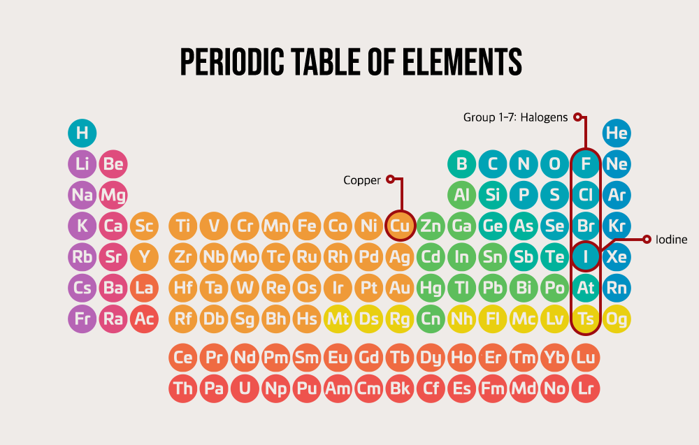
KIST researchers focused on copper iodide to overcome the weaknesses of gallium nitride and develop a new semiconductor technology that can replace it. The established theory in academia had been that substances of Group 1-7 elements of the periodic table, which includes iodine, are difficult to be used as semiconductors, since their strong electrical interactions led to high degree of interatomic bonding strength. This is because the current can flow only when the bonding strength between atoms is low enough.
However, the development of new technology opened a new horizon for semiconductor material technology research. Unlike gallium nitride, copper iodide has the weak intensity of the internal electrostatic field and high bond energy, resulting in high efficiency in photoelectric transformation – the conversion of light information into electrical signals.

Figure 3. Cross-section of a copper iodide thin film on a silicon substrate,
observed with a transmission electron microscope (TEM)
Furthermore, since the crystal structure of copper iodide is the same as that of silicon and the interatomic distance is also similar, thin films can be grown on inexpensive silicon substrates with fewer defects. The temperature for growing copper iodide thin films is also similar to the temperature for silicon device processing (below 300 °C), so it can be applied to the silicon semiconductor process without degradation.
In particular, copper iodide thin films have p-type semiconductor properties. This is a great advantage compared to the n-type semiconductor gallium nitride, which can’t be easily doped as p-type. By focusing on this point, researchers have developed a hybrid LED where n-type aluminum gallium nitride (AlGaN) and p-type copper iodide are combined together, succeeding in emitting blue light.


Figure 5. Blue light emitted from the hybrid device; the wavelength of the emitted blue light is 437 nm,
showing that the copper iodide semiconductor emits the blue light 10 times brighter than that of
gallium nitride-based devices, and that it has improved photoelectric efficiency properties and
device stability in the long term.
Since a high-performance, high-reliability blue light-emitting device can be made with copper iodide thanks to its high quantum efficiency, it is considered that CuI can be utilized to develop high-efficiency photonic devices by replacing nitride semiconductors in the future. In addition, as it can be directly grown on a large sized silicon substrate without the need for high-temperature thin film growing process and equipment, it can be used for various applications like micro-displays, which were difficult to be realized with gallium nitride.
Researchers are currently working on developing an LED consisting of copper iodide and copper chloride to enhance efficiency such as increasing the wavelength of emission. For commercialization, some challenges like improving the quality of cooper iodide thin films, optimizing the process for mass production, and the development of related equipment must be solved in advance.
With the development of this technology, it is expected that the commercial production of CuI-based semiconductors will be possible within a few years as materials for both blue and ultraviolet light sources. In particular, it is expected to play an important role as a new material for the light-emitting semiconductor that replaces gallium nitride.
1‘GaN semiconductor devices market size, share & trends analysis reports’ by Grand view research(2018)
2Efficiency levels when converting electricity into light
3A space for the electrons in semiconductors
※ This article is based on the subjective view of the contributor, and may differ from the official stance of SK hynix. Any unauthorized use of the contributor’s article may have legal responsibility.

ByDr. Joonyeon Chang
Director-General of Post-silicon Semiconductor Institute of KIST


