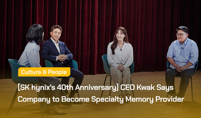
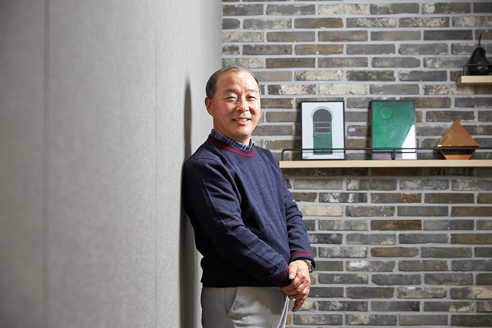
How can innovation lead to customer satisfaction? No matter how high the level of innovation is this will never be complete without consistent and reliable quality. Ensuring excellent quality and striving to further improve it is key to enhancing the value of existing products and laying a solid foundation for even greater innovation. The SK hynix newsroom team met with Sang Hoo Hong, Head of P&T, to ask him to share the philosophy and confidence that he has been keeping for over 30 years at the company.
“Complete Memory Solutions” With Precise Packaging and Strict Testing
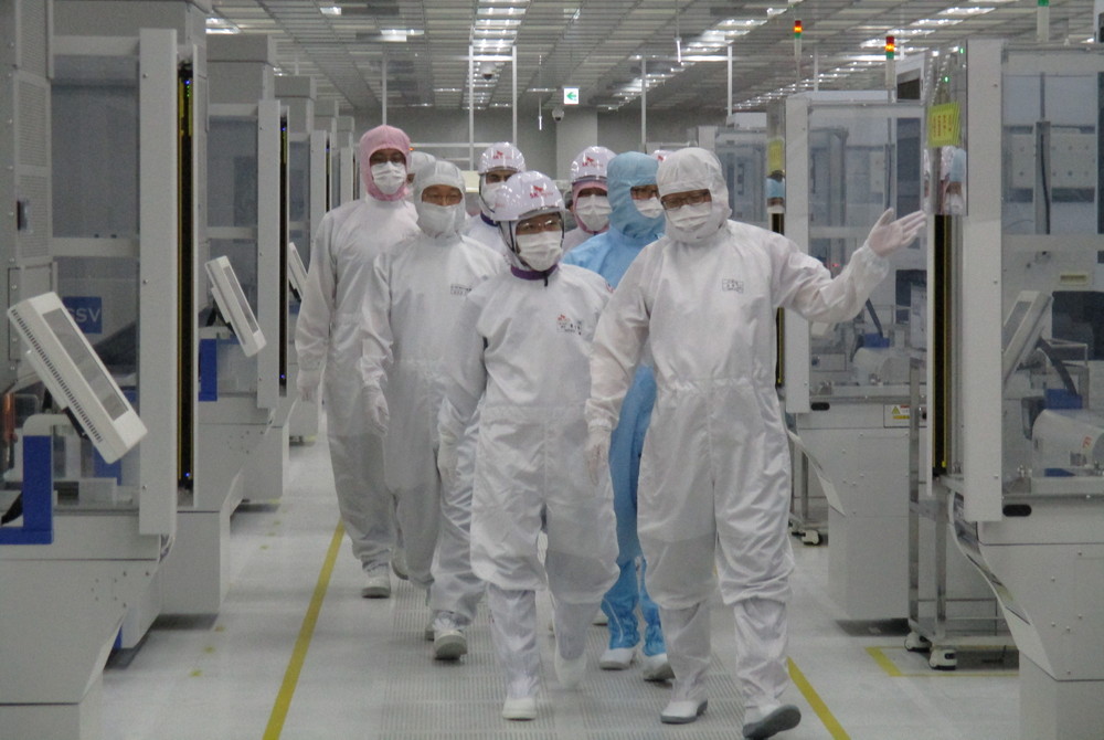
P&T stands for package and test, one of the back-end procedures of the broader semiconductor production process. During this process, wafers completed in the front-end procedure are packaged before delivery to the customers and the products go through the final test to ensure that the quality meets customer expectations. Even if a high level of quality is secured at the wafer level, there can be errors or defects depending on different customer settings. That’s why the process of completing wafers as a product and enhancing the reliability by taking into account the different circumstances of each customer is just as important as the one for product development and mass-production in fabs.
“Fab and P&T are deeply related. None of these two is less important to complete the best quality and meet customer expectations. We pay a lot of attention on communication with the fab to proactively respond to any possible issues. That is critical to faithfully fulfill the common goal of securing the utmost manufacturing competitiveness.”
One of the top priorities for the P&T team is securing technological capabilities that the market requires to boost the value of memory products.
P&T’s role was critical for SK hynix to preoccupy the market for the high-bandwidth memory (HBM), or the fastest memory available. Only those with advanced technologies and mass-production capabilities can preoccupy the market given the structure of the market. SK hynix became one of the pioneers in the market by demonstrating its capability to mass-produce HBM2E in 2019 and took over the premium memory market by initiating mass-production in full scale in July 2020.
Since the launch of the world’s first HBM in 2013, the company has made various attempts to improve product performance. This was possible thanks to P&T’s commitment for quality improvement through the innovative Wafer Level Package* technology.
“As for the HBM3’s next generation, we aim to differentiate from others in the area of high-capacity products by enhancing the speed and stacking technology. We’re particularly keen to develop equipment, special materials and process technology for this.”
Other than the cutting-edge technologies like HBM, the P&T is also continuing development of the “conventional packaging technology,” or capability to stack as many dies as possible within a package.
“Changes are gaining speed, while customers want even higher technologies over time. In one example, the NAND capacity for the latest flagship smartphones is around 256-512 gigabytes (GB), but likely to increase to 1-2 terabytes (TB) on the same density for the next-generation models. Our goal is to cut the height of a single die to below 30㎛, while increasing the number of layers, currently at eight, to 16-32 for technology competitiveness.”
With customer demands diversifying, the proportion of customized memory is increasing as well, making it more important to secure the capability to thoroughly test even the smallest specifications.
As the company accelerates its efforts to boost environmental, social and governance values as part of the broader SK Group’s “Financial Story” campaign aimed at boosting the total corporate value, Hong is also looking at ways to run the P&T manufacturing in line with the ESG management.
“For environment, we’re seeking to shift to eco-friendly materials and components, while reducing energy consumption and minimizing pollutant emissions. For example, we could save costs and reduce waste by improving the equipment for chip-making processes to replace some chemicals with eco-friendly materials. We are looking forward to finding more ways to create both economic and social values at the same time ahead.”
Leading the Way to Success
Since joining what’s formerly known as Hyundai Electronics Industries in 1986, Hong has gone through both exciting and discouraging moments of the company and now, as SK hynix thrives as one of the best semiconductor companies in the world, he is full of emotions.
“I am so grateful and relieved. We’ve come through some real difficult times such as the 1997-98 Asia financial crisis, restructuring by creditors and the 2008 global financial crisis. But look what we’ve achieved now. We’re a leading chipmaker in the world and worth over 100 trillion won in the stock market. I hope we continue to prosper, leaving all the troubles we’ve had in the past behind.”
“As one of the early members of SK hynix, I’m full of pride and confidence, but also feel heavy responsibility. Look at all the challenges we’re facing ahead. In the times of digital transformation of the 4th industrial revolution, we should successfully develop DRAM with sub- 10 nanometer (nm) level and NAND stacking technology further to beyond 600 layers as well as creating social values in the energy and environment fields.”
Innovate the Way of Working
One of the key goals for P&T this year will be to improve cost competitiveness, remove inefficiencies and bring innovation to the way of working through digital transformation and put the quality of the materials and components under control.
Over the longer term, Hong aims to further maximize the efficiency of the operation with a strategy for global integration should the process of the planned acquisition of Intel’s NAND and SSD business be complete.
Hong believes that digital transformation will accelerate establishment of Smart Factory that quickly reflects customer needs and responds to rapid changes in the industry.
“It is very important to secure the capability to effectively deal with enormous amount of data collected by P&T and build the corporate culture of making decisions based on data.”
With the portion of the younger generation in 20s-30s growing across the P&T, making his department one of the youngest parts of the company, Hong is also making various attempts to narrow potential generation gap among colleagues.
“I think providing the sense of security that you won’t be treated unfairly simply over expression of your opinion is key to communications. It’s particularly important for the younger generation as they are relatively clearer when it comes to expressions and preferences.”

“Quality” is the keyword that Hong wants to ensure that every stakeholder bears in mind.
“I’ve spent most of my time at work on improving product quality and it’s now all about what I am. Quality of the P&T, the very final stage of the semiconductor production process, leads to that of our customers’ products. For this reason, nothing can be more important than constantly improving the quality to me.
*Wafer Level Package (WLP) technology: Unlike the conventional method of cutting chips from wafers and packaging them individually, this technology allows wafers to undergo packaging and testing process as a whole before chips are cut, resulting in better performance of the products.