Conventional 3D NAND memory stores data by trapping charges in the silicon nitride film known as a charge trade nitride (CTN) layer. Despite its widespread use, 3D CTN NAND faces limitations in achieving memory expansion through cell stacking due to cell-to-cell interference and spacer oxide thickness between vertically adjacent cells. This has prompted the industry to search for alternatives to 3D CTN NAND technology that overcome these limitations, with 3D ferroelectric* NAND (Fe-NAND) emerging as a potential successor.
In 2022, researchers at SK hynix’s Revolutionary Technology Center (RTC) revealed they had demonstrated 3D Fe-NAND triple-level-cell* (TLC) operation using the ferroelectric HfO2*. This article will focus on the RTC’s latest research presented at the 2023 Very Large-Scale Integration (VLSI) Symposium, which showed 3D Fe-NAND quad-level cell* (QLC) operation for the first time using the 3D CTN NAND test vehicle*.
*Ferroelectric (FE): A material which exhibits spontaneous electric polarization without an external electrical field that can be reversed in direction by the application of an appropriate electric field.
*Triple-level cell (TLC): A form of NAND flash memory that can store up to 3 bits of data per memory cell.
*Hafnium Oxide (HfO2): A mature high-k dielectric applied to semiconductor materials due to its high dielectric constant, thermodynamic stability, and the simplicity with which it can be deposited.
*Quad-level cell (QLC): A form of NAND flash memory that can store up to 4 bits of data per memory cell.
*Test vehicle: A circuit or IC designed for the purpose of evaluating one or many device characteristics.
Finding the Ideal Cell Structure to Increase the PE Window
For 3D Fe-NAND to realize TLC and QLC operation, it required further expansion of the program/erase (PE) window*. The latest RTC research proposed novel 3D Fe-NAND cell structures that can enlarge the PE window up to 10.54 V through cell stack optimization, thereby demonstrating the feasibility of QLC operation.
*Program/erase window (PE window): The process window of erasing and writing a cell. The more P/E cycles that the NAND technology can sustain, the better the endurance of the device.
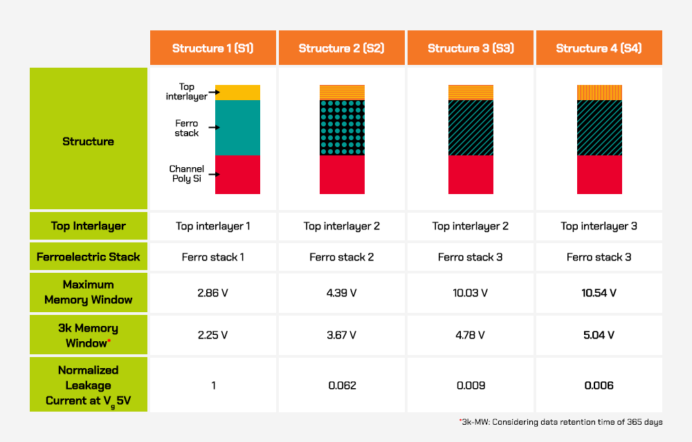
Figure 1. Table showing key characteristics of four cell stack structures (S1–S4)
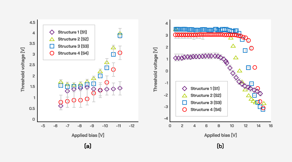
Figure 2. Graphs comparing the (a) erase and (b) program performances of S1–S4
Figure 1 summarizes the four types of cell structures (S1–S4) evaluated in this study and compares the electrical characteristics including the standard PE window, the post 3k cycle PE window, and the channel to gate leakage current. Figure 2(a) and (b) show the transfer characteristics of the four cell structures as the researchers erased and programmed the cells using the conventional ISPE* and ISPP* methods. In particular, S4 achieved the enlarged P/E window of 10.54 V by reducing the leakage current and optimizing the cell structures of the ferroelectric stack and the top interlayer.
*Incremental Step Pulse Erase (ISPE): A memory programming method in which a memory element is programmed to a specific state or set to an erase state using small, incremental voltage steps or pulses.
*Incremental Step Pulse Programming (ISPP): A memory programming method in which a series of programming pulses of increasing magnitude are applied to select memory cells to gradually raise their threshold voltage.
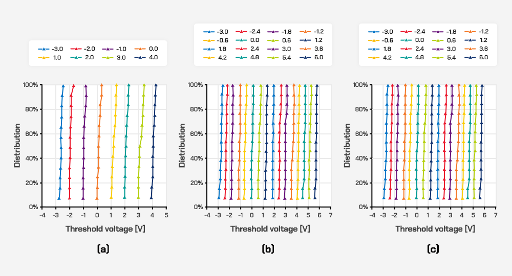
▲ Figure 3. Line graphs for S4 showing its (a) TLC threshold voltage (Vth) distribution (b) QLC Vth distribution and (c) post 3k cycle Vth distribution
Both TLC and QLC operations were performed on S4. Figure 3(a) shows TLC verification results for S4 with the minimum gap margin of 0.45 V between two adjacent threshold voltage (Vth) states. This represents a significant improvement from the RTC’s previous data, which showed a minimum gap margin of 0.11 V. Moreover, with the expanded PE window, Figure 3(b) shows S4’s QLC operation is demonstrated with the minimum gap margin of 0.24 V. In Figure 3(c), QLC Vth distribution after 3k cycling stress is shown with the reduced minimum gap margin of 0.14V. The QLC operation after the 3k cycle is verified not only by expanding the PE window, but also by improving endurance properties as a result of cell stack engineering.
3D Fe-NAND Opens the Door to a New Era
To overcome the limitations of conventional 3D CTN NAND, the researchers successfully fabricated the HfO2-based 3D Fe-NAND. The new NAND research shows that optimizing the cell stack leads to an expansion of the PE window, while the QLC operation was also demonstrated which suggests that 3D Fe-NAND is a promising potential solution in the post-3D NAND era.
For more information regarding RTC’s research, please visit the center’s research website (https://research.skhynix.com). The RTC operates the site to share insights on its ongoing research of future technologies and to actively communicate with various global research organizations.