From breaking barriers for performance with HBM3 to developing the world’s fastest mobile DRAM, LPDDR5T, SK hynix’s product portfolio is full of industry-leading solutions which have pushed technological limits. But how exactly does the company realize this rapid evolution in its solutions? What innovations and processes are applied to these products to take them to the next level?
To shed light on these technologies, SK hynix Newsroom is launching its seven-part Tech Pathfinder series. The articles in the series will introduce some of the company’s most advanced products globally renowned for their unprecedented qualities including industry-leading processing speed, data storage, and computational capabilities. Through the series, readers will gain a better grasp of the concepts behind these innovative products and gradually become more familiar with the advancement of semiconductors and technology in general.
SK hynix’s Secret Behind Its DRAM Development
In November 2022, SK hynix released a mobile DRAM with the world’s lowest operating power of 1.01-1.12V and an operating speed of 8.5 Gbps—Low Power Double Data Rate 5X (LPDDR5X). The company then made another historic step in January 2023 with the development of its Low Power Double Data Rate 5 Turbo (LPDDR5T), the world’s fastest mobile DRAM which offers an operating speed of 9.6 Gbps.

▲ Figure 1. SK hynix’s LPDDR5 Lineup Made With the HKMG Process
Smartphone mobile DRAMs need to be small, low-power devices which provide fast processing speeds to perform more functions. However, as the industry reaches the limits of scaling1, such mobile DRAM technology only becomes more complex. So, what is the secret in SK hynix’s technology that has allowed the company to remain a powerhouse in mobile DRAM development? The answer lies in the world’s first application of the High-K Metal Gate (HKMG) process to mobile DRAM. This article will summarize the principle of the HKMG process and how this technology was applied to the LPDDR5X and LPDDR5T.
1Scaling: The reduction in size of semiconductors to produce better device performance, power efficiency, and cost.
HKMG Process: Key to the World’s Fastest Mobile DRAM With Lowest-Power Consumption

▲ Figure 2. SK hynix Applies HKMG Process to Develop the World’s Fastest Mobile DRAM
Although HKMG was commercialized over a decade ago, various challenges were encountered during the development of this groundbreaking technology. There were four major obstacles: the extreme complexity of the technology, the high-processing cost compared to conventional materials, unpredictable risks, and the difficulty in controlling electron leakage. More importantly, the whole HKMG process had never been applied to mobile DRAM before. Despite facing these issues, SK hynix took on the challenge of changing the paradigm of mobile DRAMs.
More specifically, applying the HKMG process to mobile DRAM peripheral (peri) transistors posed a major challenge. DRAMs typically consist of cell transistors which store data and peri transistors which conduct data input and output. It is therefore necessary to minimize the impact of the HKMG process on the cell as the connection between the cell and peri transistor can encounter problems when applying the HKMG process to the periphery.
Accordingly, the area of the peripheral circuit that powers the cell is also reduced as the cell scale is minimized. This leads to a shrinking of the transistors that supply the charge, which, consequently, reduces the thickness of the gate insulator. These insulators for conventional mobile DRAMs are generally made from silicon oxide (SiON), which suffers from speed limitations when it is thinned. SiON also faces an efficiency problem as, when the thickness of the insulator decreases, the amount of leakage current increases and this leads to a loss in power.
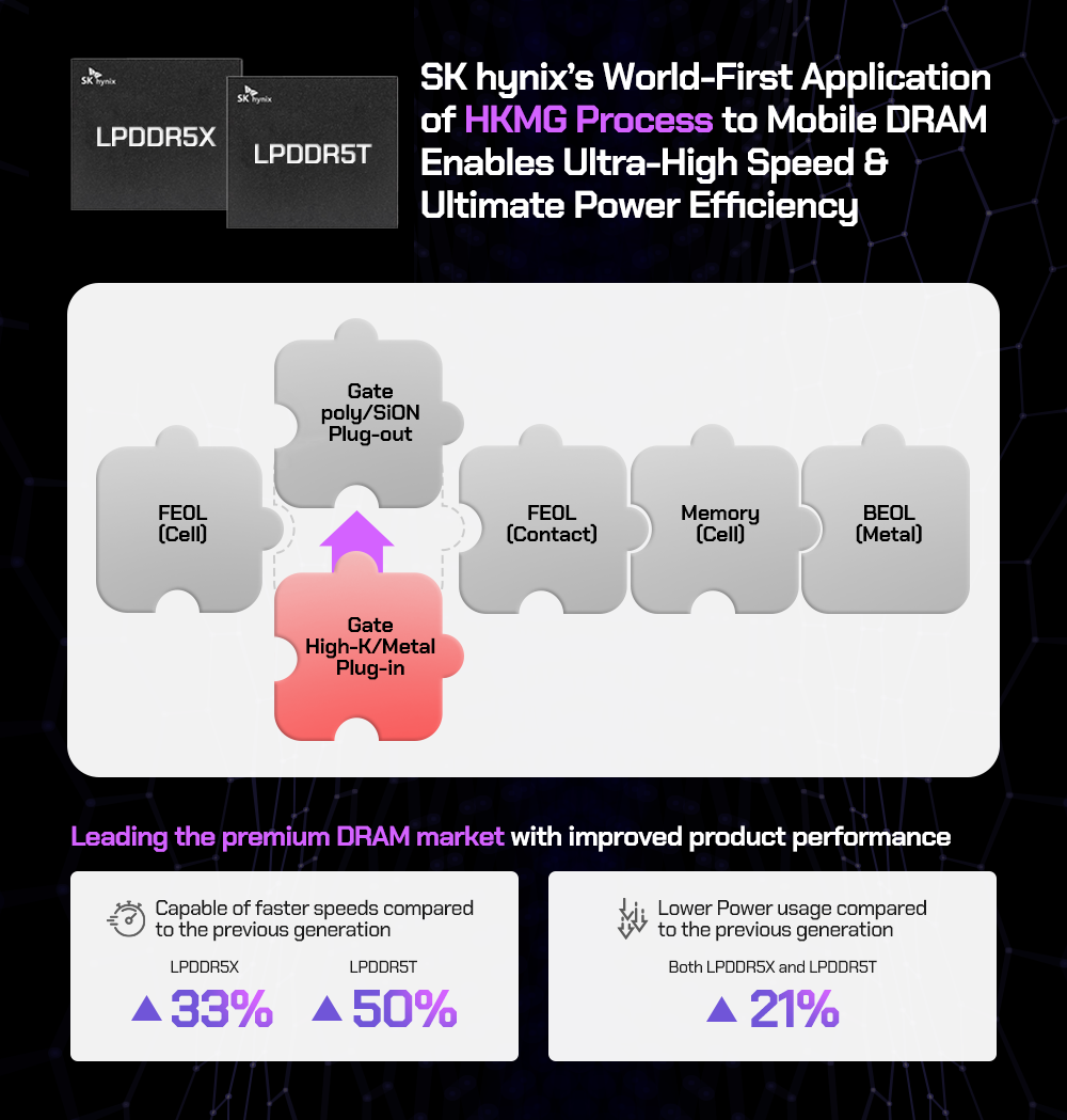
SK hynix’s solution to these issues was to apply High-K material to the insulation film as the material has a permittivity2 that is about five times higher than conventional SiON insulation film. To put this into context, when the same voltage is applied, the High-K insulation film can keep five times more charge than a conventional SiON material with the same area and thickness. This means that the thickness and leakage current can be reduced by making the insulation film with High-K material.
2Permittivity: Degree of how many electrons can be stored inside a gate.
However, the combined use of polysilicon (poly-Si)—applied in existing gates—and High-K materials increased the gate’s resistance, so a higher voltage is required and electrons slow down. To combat this, the poly-Si gate was replaced with a metal gate. With the combination of a gate oxide that possesses a high permittivity and a metal electrode, SK hynix successfully created an integrated HKMG solution.

▲ Figure 3. Description of HKMG Technology
Pioneering the Application of the HKMG Process
In preparation for the development stage, SK hynix first set up a taskforce comprised of device and process experts in the development, research, and manufacturing fields. The taskforce, the first of its kind for a derivative product3, consisted of members of the and PE (Product Engineering) team. Having begun working together from the initial stages of the process development, the taskforce resolved issues such as reliability and quality risks. Their main goal was to develop an integrated solution incorporating HKMG technology to the existing process while minimizing costs by maintaining parts of the existing process as much as possible.
3Derivative product: A product that is derived from a core product. Core products, a kind of prototype in which existing technology and elements are applied, allow manufacturers to establish a leadership position in the related technology as they can be quickly developed. The resultant derivative products feature various capacity and performance modifications to meet market needs.
It was also necessary to develop a method for utilizing the characteristics of the HKMG process to both increase speed and reduce power usage. However, due to the limitations in the chip’s size, lowering the electrical capacity to reduce power was not possible. Consequently, it became necessary to create a design that would lower the voltage. To this end, innovative design ideas were produced which eventually led to low-power solutions. These solutions included using a power architecture that would lower the design’s internal power and lowering the gate level in sleep mode to significantly reduce power consumption.
SK hynix Rewrites the Rules With LPDDR5X and LPDDR5T

▲ Figure 4. SK hynix’s World-First Application of HKMG Process to Mobile DRAM Enables Ultra-High Speed & Ultimate Power Efficiency
While effectively controlling leakage current, LPDDR5X offers a 33% increase in speed (8.5 Gbps) and a 21% power usage reduction compared to the previous generation. This increase in energy efficiency ensured the product reached its environmental goal of carbon reduction as well as meeting target technological specifications. Skip forward two months and LPDDR5T was developed. Operating in the same ultra-low voltage range as LPDDR5X, it is 13% faster at 9.6 Gbps to make it the fastest mobile DRAM available today.
SK hynix’s mobile DRAM which applies the HKMG process has been praised for its world-class performance. The company is also promoting the establishment of a new specification for mobile DRAM at the Joint Electron Device Engineering Council (JEDEC). SK hynix’s next step is to actively leverage the experience gained from the successful development of the HKMG process to bring even greater innovation to the next generation of technologies and products. In other words, LPDDR5X and LPDDR5T are just the beginning.
<Other articles from this series>


