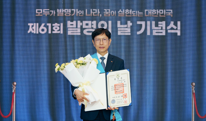


The 61st Invention Day ceremony
SK hynix announced that Ahn Hyun, Chief Development Officer (CDO), and Hyungjin Choi, Technical Leader of NAND Development received the Gold Tower Order of Industrial Service Merit and the Presidential Citation, respectively, at the 61st Invention Day ceremony, held on May 19 at COEX Magok Le West Hall in Gangseo-gu, Seoul.
Invention Day is a nationally designated commemorative day established to raise awareness of the importance of invention and inspire the spirit of innovation. On May 19 every year, the Korean Intellectual Property Office (KIPO), together with the Korea Invention Promotion Association (KIPA), holds a ceremony to recognize and honor individuals who have contributed to the nation’s industrial development through invention.


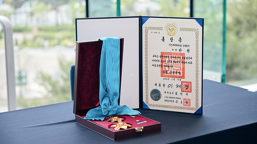
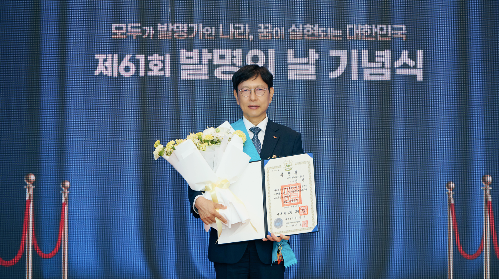
SK hynix CDO Ahn Hyun receiving the Gold Tower Order of Industrial Service Merit at the 61st Invention Day ceremony
The ceremony was attended by key government officials, including Yongseon Kim, Commissioner of the Korean Intellectual Property Office, as well as industry leaders such as SK hynix CDO Ahn Hyun. SK hynix demonstrated its elevated status as a technology leader driving Korea’s industrial development, showcasing groundbreaking innovations such as HBM4 and 321-layer 1Tb 4D NAND that have reshaped the global AI memory market.
Completing the AI Memory Portfolio to Strengthen National Semiconductor Competitiveness
CDO Ahn received the Gold Tower Order of Industrial Service Merit in recognition of his role in spearheading the development of next-generation HBM1 and elevating SK hynix’s R&D capabilities to world-class levels. He was also recognized for completing an AI memory portfolio spanning both DRAM and NAND, helping Korea secure an unrivaled position in the global AI memory market.
1HBM (High Bandwidth Memory): A high-performance, high-value memory product that vertically stacks multiple DRAM chips to increase capacity and dramatically improve data processing speed. HBM has evolved through successive generations: 1st-gen (HBM), 2nd-gen (HBM2), 3rd-gen (HBM2E), 4th-gen (HBM3), 5th-gen (HBM3E), and 6th-gen (HBM4).
“This award is an honor earned through the tenacity and boldness of all SK hynix employees, who have worked tirelessly day and night to create products and technologies the world has never seen before. Invention may begin with one person’s idea, but turning that idea into an actual product and making it an industry standard is impossible without the collaboration and perseverance of countless colleagues. In particular, HBM, invented by SK hynix, has become a key product ushering in the AI era, and I believe it serves as a valuable example of how the innovations we have built can make a significant contribution to global industrial advancement.”


SK hynix’s products on display at the 61st Invention Day ceremony
CDO Ahn played a pivotal role in the timely development of HBM4 and the establishment of the industry’s first mass production system, significantly contributing to SK hynix’s commanding share of the global AI memory market. In the NAND segment, he led the development and mass production of 321-layer 1Tb TLC2 4D NAND, opening the industry’s first era of 300-plus-layer stacking, and has been building a strong foothold in the AI data storage market on this foundation. In addition, the company developed the eSSD ‘PS1012 U.2,’ which delivers significantly improved bandwidth and sequential read speeds over the previous generation, enabling a swift response to the rapidly growing enterprise storage demand in the AI era.
2NAND flash is classified by the number of bits stored per cell: SLC (Single Level Cell, 1 bit), MLC (Multi Level Cell, 2 bits), TLC (Triple Level Cell, 3 bits), and QLC (Quadruple Level Cell, 4 bits). As the amount of stored information increases, more data can be stored in the same area.
“The HBM market is transitioning from an ‘era of standards,’ where products are supplied to predefined specifications, to an ‘era of customization,’ where we must respond swiftly to diverse customer needs. We must now evolve beyond being a product provider into a ‘Creator’ that works alongside customers from the design stage to develop optimal solutions. While SK hynix drives technological innovation in earnest, from HBM4 to Custom HBM, and further to HBF3 and 3D Stacked DRAM on Logic4, we will continue to maintain our overwhelming technological lead in the global AI memory market.”
3HBF (High Bandwidth Flash): A next-generation NAND solution with enhanced ultra-high-speed data transfer capabilities, designed to efficiently process the surging volume of large-scale computational data (such as KV Cache). Like HBM, it applies logic processing to the base die to maximize performance.
43D Stacked DRAM (3D Stacked DRAM on Logic): A cutting-edge stacking technology that vertically stacks DRAM directly on top of logic semiconductors such as SoC (System on Chip). By significantly increasing data pathways (I/O), it minimizes latency and dramatically improves power efficiency and space utilization, making it particularly suited for on-device AI applications.
CDO Ahn has also devoted significant effort to securing next-generation memory technologies. Through a strategic partnership with NAVER Cloud, he applied CXL5 and PIM6, which are often considered as next-generation memory technologies, to real-world service environments, verifying their performance and advancing system optimization. The company has also completed customer certification for its CXL 2.0-based ‘CMM (CXL Memory Module)-DDR57’ and is progressing smoothly toward commercialization.
In the NAND segment, SK hynix is pursuing its ‘AI-NAND Family’ strategy, developing next-generation products specialized for each application area, including ‘AIN-P,’ a next-generation high-speed eSSD NAND, and ‘AIN-B,’ which leverages TSV technology to secure high bandwidth, laying the technological groundwork for future AI infrastructure. Notably, AIN-B is being brought to market under the product name HBF through a strategic partnership with SanDisk, with both companies jointly working on technical standardization.
5CXL (Compute eXpress Link): An interface technology that efficiently connects memory, processors, and other components within a system, extending the limits of bandwidth and capacity.
6PIM (Processing-In-Memory): A next-generation memory technology that adds processor-level computational capabilities to memory, eliminating the data bottleneck between memory and processors and dramatically improving performance.
7CMM-DDR5: A product that expands system capacity by 50% and bandwidth by 30% compared to conventional DDR5 modules, achieving data processing capability of 36GB per second. It is regarded as a key memory solution for the upcoming AI cloud era.
Furthermore, SK hynix established the world’s first mass production system for ‘ZUFS8 4.1,’ driving technological innovation in the mobile AI segment. The company also became the first Korean semiconductor company to obtain ‘ASPICE9 Level 2’ certification last year, laying the technological foundation for its push into the global automotive market.
8ZUFS (Zoned Universal Flash Storage): An advanced version of UFS, a flash memory product used in electronic devices such as digital cameras and mobile phones, featuring enhanced data management efficiency. The product stores and manages data with similar characteristics in designated zones, optimizing data transfer between the operating system and the storage device.
9ASPICE (Automotive Software Performance Improvement and Capability Determination): A standard that evaluates and officially grades the capabilities of suppliers that provide components to automakers, with the goal of improving their quality competencies.
“To address the ‘Memory Wall,’ the most fundamental challenge facing the AI industry today, we must simultaneously innovate across three pillars: bandwidth, capacity, and power efficiency. This requires moving beyond a view of DRAM, NAND, and solutions as individual products and instead adopting a holistic approach that integrates them into a ‘single unified memory stack’ designed to maximize system-level performance. We will continue to think critically and push boundaries, working to establish the standards for next-generation AI infrastructure.”
Beyond these achievements, CDO Ahn has also been actively strengthening supply chain competitiveness through technology partnerships with academia and small-and-medium enterprises. He leads global research organizations across the United States, Taiwan, and Europe, and is building a global talent network to secure next-generation semiconductor talent.
“The semiconductor industry is not built by one company’s technology alone — it is an industry shaped by an entire ecosystem encompassing diverse partners. No matter how outstanding the technology, it can never be turned into a finished product without trusted partners and the talent to bring it to life. Going forward, we will continue to view our partners not as just ‘suppliers’ but as ‘partners growing together with us,’ and we will work to build a resilient industrial structure that can withstand external uncertainties. We will also connect R&D hubs around the world and dedicate ourselves to cultivating future talent, building the global technological capabilities needed to shape the AI era together.”
“We Will Solidify Our Leadership in the Global AI Memory Market Through Technological Innovation”
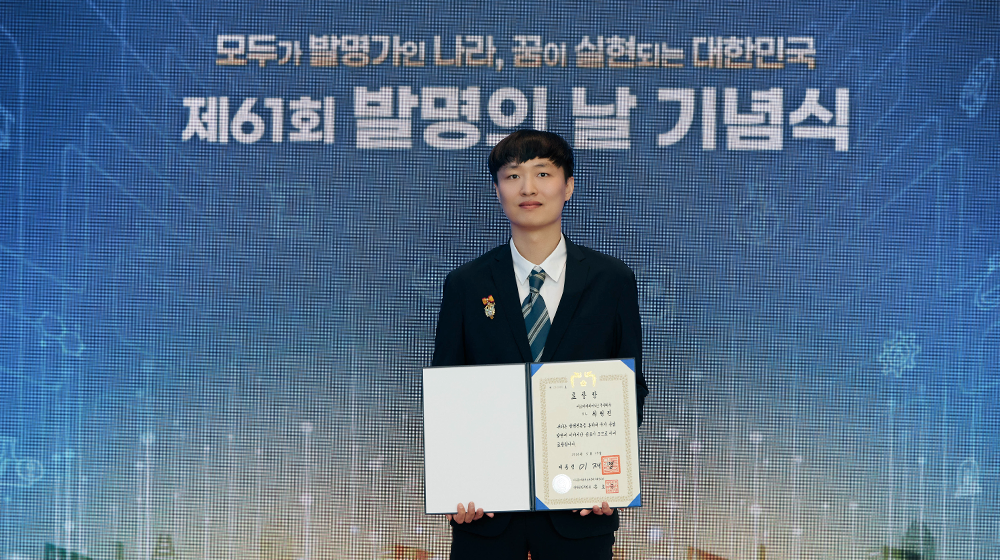
Technical Leader Hyungjin Choi received the Presidential Citation for securing core 4D NAND technologies through patents and developing the high-capacity NAND essential for AI, thereby achieving industry-leading cost competitiveness and performance. He proposed a technical idea that innovatively reduced the area of peripheral circuits essential for 4D NAND operation without requiring any additional equipment, dramatically improving cost competitiveness. He also introduced proprietary operational technologies that significantly reduced power consumption during data read and write operations while enhancing product reliability, playing a key role in SK hynix’s achievement as the first in the industry to develop and establish a mass production system for 321-layer 4D QLC NAND.
In addition, he identified a number of new technical ideas for applying the MSC10 structure — capable of surpassing the limitations of conventional single-cell-based architectures — to actual designs, contributing to SK hynix’s preemption of PLC (Penta Level Cell) technology, the next generation after QLC (Quadruple Level Cell). Beyond this, Technical Leader Choi continues to secure patents essential for next-generation memory NAND and has also been active in training researchers, contributing to the enhancement of SK hynix’s overall R&D capabilities.
10MSC (Multi Site Cell): A cell structure that reduces the area of a single cell to create two cells, with each cell distinguishing six data values.
“I am very pleased that this award has recognized the value of the intellectual property we have built through years of intense effort and dedication. I am especially proud and gratified that the ideas of myself and my colleagues have contributed, even if in a small way, to the company’s achievement of opening the industry’s first era of 300-plus-layer stacking. I will continue to pursue research and development without resting on our current achievements, driven by the desire to earn this kind of fulfillment again.”
SK hynix described this recognition as going beyond individual achievement, calling it “a result born from one team-based technological innovation that the company champions.”
SK hynix stated, “This recognition reaffirms the technological achievements SK hynix has built in the AI memory market and Korea’s elevated standing in the global semiconductor landscape.” The company added, “We will continue to accelerate the development of next-generation AI memory to solidify our global technology leadership and remain committed to intellectual property creation and the advancement of mass production technologies, driving mutual growth with the domestic semiconductor ecosystem.”