A premium, high-performance technology which has revolutionized data processing speeds by vertically stacking multiple DRAMs using through-silicon via (TSV)1—it is none other than High Bandwidth Memory (HBM). This groundbreaking memory solution utilizes an advanced packaging method to vertically interconnect the upper and lower chips through thousands of microscopic holes in the DRAMs. Through this process, the performance of the HBM product is increased while its size is reduced.
1Through-silicon via (TSV): A type of vertical interconnect access (via) that completely passes through a silicon die or wafer to enable the stacking of silicon dice.
As a next-generation memory technology, HBM offers solutions to key problems faced in the memory sector. In the video above, a data bottleneck is demonstrated by the long line of people—representing data—standing at the platform of D (DRAM) Station. So, what causes data to be stuck at a standstill like this?
To provide some context to this issue, it is necessary to know that there are eight DQs2, or paths for data input/output, per chip in a typical DRAM. When organized into units of DIMM3 modules, there are a total of 64 DQs. However, as system requirements for DRAMs and processing speed have increased, the amount of data being transferred has risen as well. Consequently, the number of DQs—the number of entrances and exits at D Station—was no longer sufficient for the smooth passage of data.
2DQ: A path for data transfer that acts as the data bus for the communication between the processor and memory. It has the characteristic of being bidirectional as it must be capable of both reading and writing.
3Dual in-line memory module (DIMM): A memory module that is mounted on a printed circuit board and contains multiple memory chips. It is usually used as a primary memory unit in a PC or server.
HBM is the solution for such data bottlenecks. It has a whopping 1,024 DQs and its form factor, which refers to the physical area, is more than 10 times smaller than a standard DRAM thanks to SIP4 and TSV technology. As a vast amount of space is required for conventional DRAMs to communicate with processors like CPUs and GPUs since they need to be connected through wire bonding5 or PCB traces6, it is impossible for DRAMs to conduct parallel processing for large amounts of data. In contrast, HBM products can communicate over very short distances which allows for the increase in DQ paths. These HBM technologies dramatically increase the movement of signals traveling between stacked DRAMs and enable data transfer at high speeds with low power consumption.
4System-in-package (SIP): A type of package in which multiple devices are made into a single package to implement a system.
5Wire bonding: A method for creating electrical interconnections between electrical device components.
6PCB trace: An electrical connection formed on a printed circuit board.
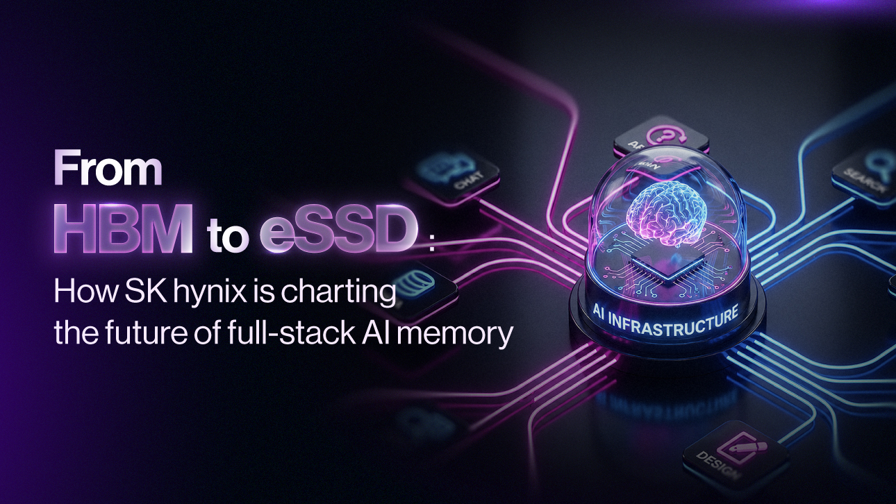
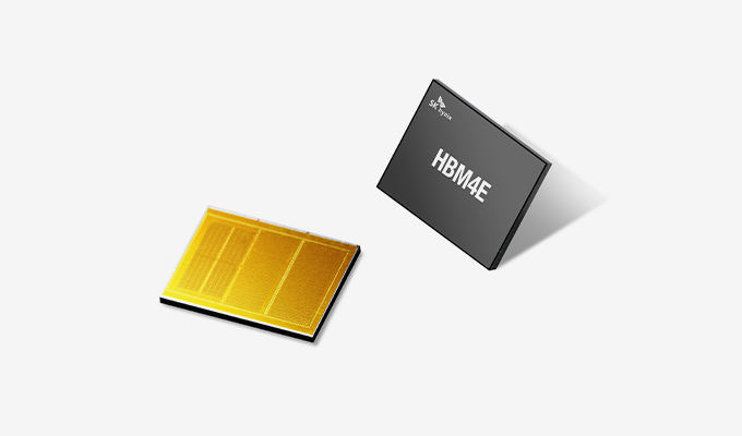
SK hynix, which developed the industry’s first HBM in 2013, began mass production of HBM3 in June 2022. As the fourth generation of HBM, HBM3 is approximately 78% faster than its predecessor, HBM2E. With such capabilities, HBM products can be deployed in high-performance data centers and applied to machine learning, supercomputers, artificial intelligence systems, and other advanced technologies.
SK hynix will continue to develop HBM products while ensuring that all its solutions adhere to ESG management standards to maintain its position as a leader in the premium memory market.
<Other articles from this series>
[We Do Future Technology] Become a Semiconductor Expert with SK hynix – AI Semiconductors
[We Do Future Technology] Become a Semiconductor Expert with SK hynix – UFS