When an object called “semiconductor” is defined, it is usually interpreted literally. As a word combining a prefix “semi-” meaning “half” with the word “conductor”, semiconductor means “half conductor”, an intermediate form of conductor and insulator. Then, what exactly does it mean to say that an electric current flows in “half”? How can we define it more precisely?
1. Semiconductors from the Perspective of Current
The criterion that distinguishes between conductors and insulators is the “flow of current”. If a current flows, it is a conductor, and if it doesn’t, it is an insulator. Then, how much current should flow exactly in a semiconductor, as a concept between a conductor and an insulator? 10 [A] or 10 [mA]? 10 [nA] or 10 [pA]? No one can give the right answer to this. This is because the meaning of “an electric current flows in half” is only literary rhetoric, and is not defined scientifically.
Nevertheless, dichotomous rules such as “flowing (ON)” and “not flowing (OFF)” make sense both literally and scientifically, so it is reasonable to define conductors and insulators. In this sense, semiconductors, meaning half-“flowing”, are included in the “flowing (ON)” category, so they should be considered as “conductors”. Thus, in terms of current, semiconductors would have to be included in the category of conductors. Then, what is the reason for distinguishing semiconductors from conductors?
2. “Doping” to Change Insulating Material to Conductive Material
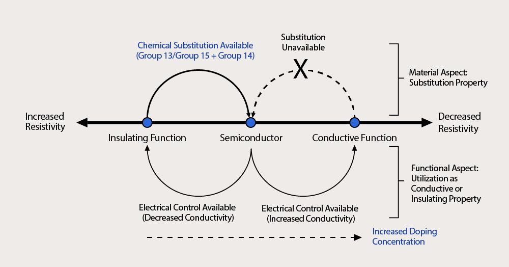
▲ <Figure 1>Correlation of insulating and conductive functions of semiconductors according to changes in resistivity (Refer to the book “Basic Insight NAND Flash Memory” by Jong-moon Jin)
The reason is that, when it comes to distinguishing between conductors, semiconductors, and insulators, the influence of the “material property” is greater than the influence of properties or operations of the object. Among the materials on Earth, especially pure germanium and silicon, which are Group 14 elements, are insulating materials; however, when a Group 13 or Group 15 element is chemically mixed (doped) with a Group 14 element and bonded with the Group 14 element (sharing atoms and outermost electrons), the conductivity (σ) increases. In other words, the resistivity (ρ), which means the degree to which electricity cannot pass through, decreases accordingly. It means a breakthrough technological innovation where the amount of current can be controlled as desired while managing the doping concentration freely at the same time. As this shows, the charm of semiconductors is that they convert pure silicon insulators into conductive materials through doping (diffusion or ion-implantation method).
At this time, the conductivity or resistivity is determined according to the doping amount, and the material doped to have a medium resistivity value lower than an insulating material and higher than a conductive material is called a semiconductor. This material has many types such as a substrate (N-type/P-type substrate), a well (N-type/P-type), a source/drain terminal (N-type/P-type), a poly-gate terminal, and other minor layers. Semiconductors are sometimes used as conductive objects or insulating objects. For this reason, defining semiconductors as a material used as a “half conductor” is rather vague. From three to four years ago, a material called CTF with a concept of half conductor is sometimes used when confining (storing) electrons in 3D-NAND, but except for these cases, semiconductors function as conductors or insulators.
3. Resistivity for Distinguishing between Conductors, Semiconductors, and Insulators
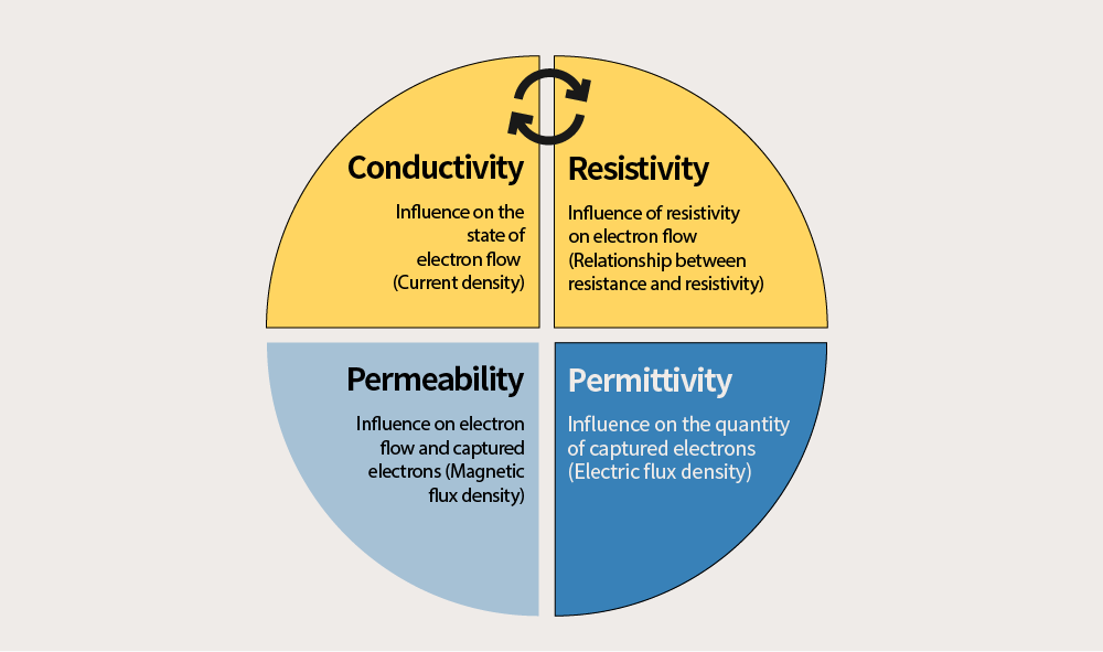
▲ <Figure 2>Four constants affecting semiconductors
Semiconductors can be expressed and classified by many variables and constants, but it is convenient to express them with constants when distinguishing the material property from insulators or conductors. Among various constants to describe a semiconductor, conductivity, permittivity, or permeability that are considered in the semiconductor is complicated in that electrical or magnetic properties should be derived by inputting variables (variables such as the strength of electric field or magnetic field).
When using the constant ρ of the resistivity <R=ρ (length/area)>, however, the three-dimensional volume (length and area) and material properties of a semiconductor can be derived from fixed values (constants). Also, it has the advantage of not being easily influenced by other values other than temperature. The resistivity of semiconductors can be classified in a range of 10^-4 to 10^2 Ω⋅m, which makes it convenient to express the properties of the material (The ranges are slightly different by data); however, these resistivity values are also variable with the changes in temperature.
4. What is a Semiconductor?
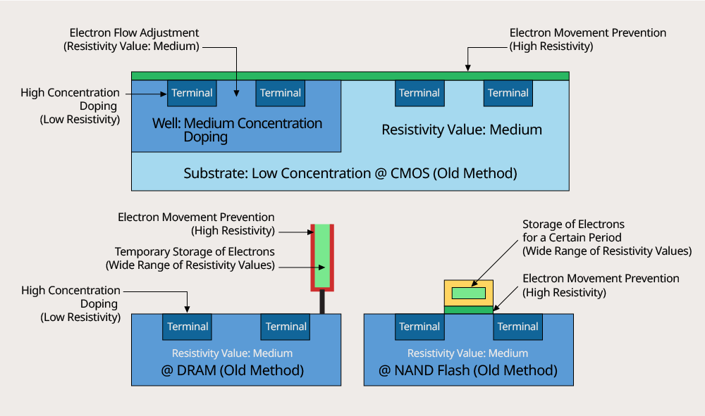
▲ <Figure 3>Internal structure of TR and resistivity @ Old model structure
In conclusion, a semiconductor is an object with a lowered resistivity constant of the material to about 10^-4 to 10^2 Ω⋅m by chemically bonding (doping) impurity elements of Group 13 or Group 15 to pure silicon, an insulating material. This doping method determines the resistivity or conductivity constant of both non-memory and memory devices by allowing each material or layer to have its own constant. The charge moves easily or hardly according to the extent calculated in advance by the values of these constants, which also affect the ability to capture or store electrons. Memory devices are also influenced by dielectric constant (proportional charge accumulation) or permeability constant (proportional magnetic flux density).
Therefore, the quantity of drain current and the number of electrons captured in the capacitor of a DRAM and the floating gate of a NAND are determined by adjusting the four constants mentioned – resistivity, conductivity, permittivity, and permeability. Also, the influence of the external current flow on the captured or flowing electrons should be minimized (By calculating the value and changing the structure or material accordingly, the flow of electrons and the number of electrons are prevented from experiencing rapid changes). Eventually, by adjusting the amount of doping and structural forms that change the material of a layer, the four constants have appropriate values so that the device made by combining semiconductors can perform the function of ON/OFF properly.
Insulators have various materials such as oxidized materials, nitride materials, and silicon-based materials (gallium arsenide semiconductors, etc.). Among them, semiconductors made of a material with the desired conductivity through doping on an insulator of a pure silicon material are representative. Once doping is performed, the doping amount doesn’t change, and the “resistivity” value is fixed in reverse proportion accordingly. In short, a semiconductor can be explained as a conductor where the resistivity value has been changed by doping impurity of Group 13 or Group 15 in insulating silicon. There is no semiconductor which is a half conductor. While alchemy to convert non-gold materials to gold eventually had failed despite countless attempts for a long time, it can be said that a kind of transformed alchemy of the 20th century has succeeded with the birth of doped semiconductors.

By Jong-moon Jin
Teacher at Chungbuk Semiconductor High School