

The “encapsulation process”, which encapsulates packages, is a step where a semiconductor chip is wrapped with a certain material to protect it from the external environment. It is also a step that reveals the characteristics of “light, thin, short, and small”, which packages aim for. The encapsulation process can be largely divided into a hermetic method in which a ceramic plate or a metal lid is attached to seal, and a molding method in which a plastic epoxy material is melted and cured to seal. Of these two, the hermetic method is rarely used currently while the molding method using epoxy molding compound (EMC) is generally and more widely used. The molding process can be divided again into transfer molding and compression molding, according to the method of filling the semiconductor with resin. Today, we will briefly take a look at the encapsulation process and then learn about molding methods in detail.
※ Encapsulation, sealing, airtight sealing, etc. have similar meanings. In this article, encapsulation is regarded as a concept of a larger category, and sealing is limited to molding.
1. Package Encapsulation Method by Encapsulant

Figure 1. Comparison between hermetic method and molding method
Packages encapsulated in a hermetic method using ceramic or metal have the advantage of being durable with a long life. For this reason, this method is mainly applied to devices in special fields, such as national defense and medical care. Representative product types include CPU, Erasable Programmable Read-Only Memory (EPROM, non-volatile semiconductor memory chip), and Power TR (large output transistor used for power).
The hermetic method is highly reliable but it is expensive. For this reason, the molding method using a plastic epoxy material is widely used. In the case of plastics, the range of use is rapidly expanding with the continuous improvement of defects such as moisture and internal voids. From EPROM, plastic materials are used for sealing in almost all cases and are applied to most packages including DRAM, CPU, and NAND.
To give a simple explanation for understanding, the hermetic method is like the method of attaching concrete panels made in advance at the factory to the exterior wall of a building, while the molding method is like the method of making a formwork and pouring concrete at the construction site. While the molding method is a method with improved flexibility, the possibility of pores occurring in the concrete is higher than the hermetic method.
2. Molding Material: Epoxy Molding Compound (EMC)
Epoxy molding compound (EMC), one of the essential functional materials required for the semiconductor back-end process, is a type of plastic. EMC consists mostly of a resin-based material, and the rest is composed of a mixture of filler and hardener. Epoxy in a powder compound form melts and becomes less viscous when dissolved into a gel state at a temperature of 175℃. When the temperature is lowered after, the epoxy cures, and the viscosity starts to increase in inverse proportion to the temperature. When the temperature is further lowered at this point, the epoxy shows strong bonding strength with the surrounding printed circuit boards (PCBs), lead frames, wires, wafers, etc., and becomes a material with a very high level of hardness. This material is called a thermosetting epoxy. After curing, it is important to control the EMC to consistently expand and contract similar to the chip when the temperature fluctuates, while the semiconductor is operating. Also, it is important to let the heat dissipate to the outside. Therefore, it can be said that the properties of the mixture determine the reliability of EMC.
3. Type of Molding Process
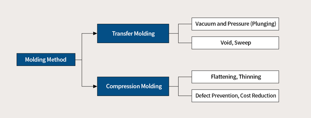
Figure 2. Molding process: transfer molding and compression molding
Molding means making something into a certain shape. When molding a semiconductor, EMC is melted and injected into the cavity. The key of a molder, the machine responsible for molding, is the molder plate. Molding methods include transfer molding, which is an old method, vacuum molding, which is an advanced method that compensates for the disadvantages of transfer molding, and compression molding, which faces down the wafer vertically.
3-1. Transfer Molding
![]()
Figure 3. Transfer molding
Transfer molding uses resin, as an early method of molding. In this method, the epoxy is melted in a gel state and then a certain pressure (plunging) is applied forcibly to allow it to move through multiple narrow paths. As chips became smaller and more multi-layered, and the wire bonding structure became more complex, the epoxy could not spread evenly during molding, causing incomplete molding or increased occurrence of voids or porosities. In other words, controlling the speed of epoxy became more difficult.
To solve this problem, when moving the epoxy through a narrow path, a method of creating a vacuum and pulling it out from the other side is used to control the speed of the epoxy. Also, various efforts are being made to reduce voids by allowing the epoxy to spread evenly.
3-2. Compression Molding

Figure 4. Compression Molding
As the number of chip layers increased (Multi Chip Package, MCP) and wire bonding became more complicated, transfer molding gradually revealed its limitations. In particular, due to the larger size of carriers (PCBs or lead frames) for cost reduction, transfer molding became more difficult. Along with this, as it was difficult for the epoxy to penetrate the complex structure and spread further, a new method was needed.
Compression molding is a new method that overcomes the limitations of transfer molding, as a method in which EMC is first placed in a mold and then melted. When applying the compression molding method, there is no need to transfer the epoxy far away. It is a method of molding by vertically lowering (facing down) the wafer on the epoxy in a gel state. This method reduces defects such as voids and sweep phenomena and is positive for the environment by reducing the unnecessary use of the epoxy.
For molding the semiconductor by using epoxy, the transfer method and compression method are being used together. The compression method is highly preferred by suppliers for its advantages such as defect detection, cost reduction, and minimization of environmental impact. As customers’ needs for product flattening and thinning are increasing, it is expected that the compression method will be used more actively in the future.

ByJong-moon Jin
Teacher at Chungbuk Semiconductor High School


