

Patterning processes include exposure, development, etching, and ion implantation. Among them, the etching process is a step to remove the lower part of the layer not covered by the photoresist (PR) following the photo process with an aim to leave the necessary pattern only. It is a process where the mask pattern is lowered onto the wafer coated with PR (exposure → development) and the PR pattern is transferred back to the layer formed under the PR. As the critical dimension (CD) of circuits became miniaturized (2D perspective), the method moved from wet etching to dry etching, leading to greater complexity of equipment and processes. The etching process saw fluctuations in the core performance index due to the active adoption of the 3D cell stacking method and it has become one of the key processes for semiconductor manufacturing along with the photo process.
1. Trend of Technological Development of Deposition and Etching
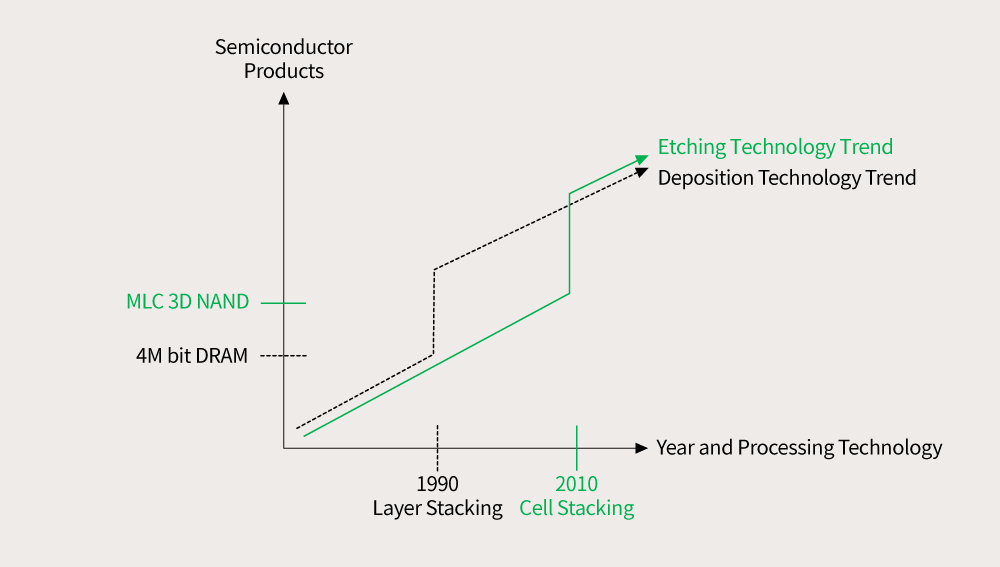
Figure 1. Trend of technological development of deposition and etching
The process of forming a layer on a wafer is called deposition (CVD, ALD, and PVD) and the process of drawing a circuit pattern on the layer formed is called exposure. Etching is a process of carving the patterns on the wafers following the deposition and exposure processes. Since the photo process is like drawing a rough sketch, what really brings an apparent change to the wafers are deposition and etching processes.
There have been significant developments in both etching and deposition technologies since the birth of semiconductors. The most remarkable innovation in deposition technology was moving to a stacking method from a trench method in accordance with greater capacity of devices from 4 Megabit (Mb) DRAM from 1Mb in early 1990s. A pivotal moment for the etching technology was in early 2010s when 3D NAND flash cells were stacked in more than 24 layers. With the number of layers having increased to 128, 256, and 512 afterwards, etching has become one of the most technically difficult processes.
2. Changes of Etching Method

Figure 2. Development of etching method along with miniaturization (2D)
The etching process has developed in accordance with the miniaturization progress of 2D (planar structure) semiconductors and the development of the stacking technology of 3D (spatial structure) semiconductors. In the 1970s, when 2D semiconductors were the mainstream, the circuit CD was rapidly decreasing from 100 micrometers (㎛) to 10 ㎛, or even lower. During this time, most of the line-up of the key process technologies of semiconductor manufacturing was finalized, while the transition of the etching technology from wet etching to dry etching was complete. For layer-cutting technology, chemical wet method, a relatively easy technique, was the first to be applied. As meeting the requirements for the 5 ㎛ of CD was difficult with the chemical wet method from early 1970s, a dry method using plasma was developed. Today, the dry method accounts for most of the etching process, while wet etching technique was later adopted and developed for the cleaning process.
3. Strengths and Weaknesses of Wet Etching and Dry Etching
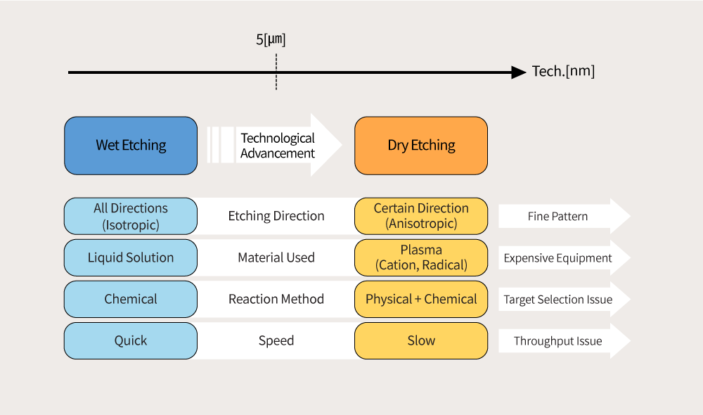
Figure 3. Strengths and weaknesses of wet etching and dry etching
With usage of a liquid, wet etching is faster, removing a greater depth per minute, but doesn’t result in a straight square-like structure. It etches all directions evenly. This leads to a loss in the lateral direction, which should be avoided for miniaturization of CD. On the contrary, dry etching allows cutting in a certain direction, making realization of the ultra-fine profile of the intended nanometer (nm) level possible.
Also, wet etching results in pollution since the used liquid should be discarded after the completion of the process. In contrast, dry etching uses a device called a scrubber in the middle of the discharge line to neutralize the exhaust gas before discharging into the air, resulting in less impact on the environment.
Meanwhile, since multiple layers are complicatedly intertwined on a wafer, it is difficult to target a certain layer (film) during etching. Wet etching is an easier option when targeting a certain film as it uses chemical reaction. It’s not easy to apply the dry method for selective etching as it’s a combination of physical and chemical techniques.
4. Etching Process Flow and Related Issues

Figure 4. Etching-related process flow
The flow of the process starting from forming a film, applying PR on it and going through various steps like exposure, development, etching, ashing, cleaning, inspection and ion implantation is to create three TR terminals, the core process for semiconductor manufacturing. If the process of cutting the PR during the development step doesn’t go well, the remaining PR hinders etching. If a targeted layer is not sufficiently etched during the etching process, ion cannot be implanted as planned as impurity particles block. The same applies if the polymer residue remaining after dry etching is not thoroughly cleaned. If the amount of plasma ion gas is too large or a film is over-etched, due to a failure in time control, physical damage is caused on the lower film.
For this reason, it is crucial to find a precise end of point (EOP) in dry etching. It’s also important to thoroughly check the etching condition as well as the ashing and the cleaning process. A wafer could be rejected if it’s unevenly etched and under-etching is more fatal than over-etching.
Since the etching process involves complicated steps, I intend to divide the coverage into two parts. In this part, we’ve gone through the overall history and the direction of the etching technology development. We’ll look into more details of the relation between plasma and etching, RIE, one of the etching methods, the Aspect Ratio and the speed of etching in the next part.

ByJong-moon Jin
Teacher at Chungbuk Semiconductor High School


