

Wet etching of the early days has led to the development in the cleaning or ashing process and dry-etching method using plasma has settled as the mainstream. Plasma consists of electrons, cations, and radical particles. The energy applied onto the plasma removes the outermost electrons of the source gas in neutral state to turn them into cations. It also removes imperfect atoms from the molecule to form radicals in the electrically neutral state. Dry etching uses cations and radicals that constitute plasma where cations are anisotropic (etching in a certain direction), and radicals are isotropic (etching in all directions). There are far more radicals than the amount of cations. In this case, dry etching should be isotropic like wet etching, but it is anisotropic etching that enables ultra-miniaturized circuits. Why? Also, the etching speed of cations and radicals is very slow, then how can we apply plasma to etching for mass production despite this disadvantage?
1. Aspect Ratio (A/R)

Figure 1. Concept of aspect ratio and changes in aspect ratio in accordance with technological advancement
Aspect Ratio (A/R) is the ratio of the horizontal axis length compared to the vertical axis (height divided by width). As the critical dimension (CD) of a circuit gets smaller, the A/R value increases. That is, if the width is 10 nm when the A/R is 10, a hole with a 100 nm height should be dug out in the etching process. Therefore, for next-generation products requiring ultra-miniaturization (2D) or high density (3D), an extremely high A/R should be achieved to allow cations to penetrate the lower layer during etching.
To implement ultra-miniaturization technology with a CD less than 10 nm in 2D, the capacitor A/R of DRAM should be kept above 100. Likewise, the 3D of NAND flash also requires a high A/R to stack 256 layers or more of cells. Even if the required conditions of other processes are met, the necessary product cannot be produced unless the etching process supports it. This is why etching technology is becoming more important.
2. Overview of Plasma Etching

Figure 2. Plasma source gas by film type
When a tube is hollow, the narrower the diameter of the tube is, the easier it gets for the liquid to enter due to the capillary phenomenon. However, it gets rather difficult if you have to dig out a hole (dead end) in the bare ground. For this reason, since the mid-70s when the circuit CD was 3 to 5 ㎛, dry etching became the trend, replacing wet etching. That is, although ionized, it is much easier to penetrate deep holes since the volume of individual molecules is smaller than that of organically agglomerated solution molecules.
In plasma etching, the inside of a process chamber where etching is to be performed should be first made into a vacuum state, before a plasma source gas suitable for the layer is injected. When etching a solid oxide film, a strong C-F-based source is used. For silicon or metal films, which are relatively weaker, a CL-based source gas is used.
Then, how should the gate layers and the underlying silicon dioxide (SiO2) insulating layers be etched?
First, in the case of gate layers, silicon is removed with a CL-based plasma (Si+ Cl2) with an etch selectivity of polysilicon. For the lower insulating layer, a two-step etching is performed with a more powerful C-F-based source gas (SiO2+CF4) with the selectivity to etch the SiO2 film.
3. Reactive Ion Etching (RIE, or Physicochemical Etching) Process
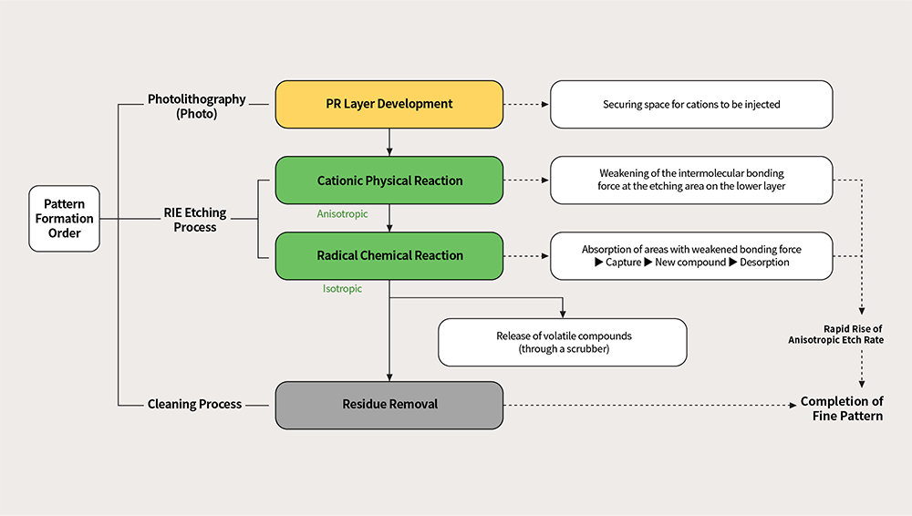
Figure 3. Strengths of RIE method (anisotropy and high etch rate)
Plasma contains both isotropic radicals and anisotropic cations at the same time, then how does it perform anisotropic etching?
Dry etching using plasma is mostly performed in the reactive ion etching (RIE) method or an application based on the RIE method. The core of the RIE method is to weaken the binding force between the molecules of the target in the film by attacking the etching area with anisotropic cations. The weakened area is absorbed by radicals, combined with the particles constituting the layer to make them into a gas, which is a volatile compound, and release.
Although radicals are isotropic, molecules that make up the bottom surface, whose bonding force is weakened by the attack of cations, are more easily captured by radicals and turn into new compounds, than the walls with a strong bonding force. Therefore, downward etching becomes the mainstream. The captured particles turn into a gas with the radicals and are desorbed from the surface and released by the force of vacuum.
At this time, when physicochemical etching is performed by combining cations acting physically and radicals reacting chemically, the etch rate (etching degree over time) increases by 10 times compared to the case of performing cation etching or radical etching separately. With this method, the etch rate of the anisotropic downwards etching increases, resolving the issue of the polymer remaining after etching at the same time. This method is called RIE etching. The key to a successful RIE etching is to find the right plasma source gas suitable for the film to be etched. Note: Since plasma etching is RIE etching, they can be considered as the same concept.
4. Etch Rate and Core Performance Index

Figure 4. Core etching performance index related to the etch rate
The etch rate refers to the depth of a hope when etching a film for one minute. Then, what does it mean that etch rates of various parts on a single wafer are different from each other?
This means that the depth of etching is different for each point on the wafer. For this reason, it is important to set the end of point (EOP) where etching should be stopped by considering the average etch rate and the depth of etching. Even when an EOP is set, there are still areas that are overly etched (over-etching) or insufficiently etched (under-etching) than planned. In etching, however, over-etching causes less damage than under-etching. This is because the less etched part in the case of under-etching hinders the following process such as ion implantation.
Meanwhile, selectivity, measured by etch rate, is a key performance index for etching. The criterion is the etch rate of the target layer compared to the etch rate of the layer that always plays a role in masking (PR film, oxide film, nitride film, etc.). This means that the higher the selectivity is, the faster the target layer is etched. The higher level of miniaturization requires a higher selectivity so that fine patterns can be properly realized. The selectivity of cationic etching is low since the direction is straight, but the selectivity of radical etching is high, resulting in the increased selectivity of RIE.
5. Etching Process

Figure 5. Etching Process
First, a wafer is placed in a furnace of the oxidation process where the temperature is kept between 800 to 1,000 degrees Celsius, and then a silicon dioxide (SiO2) film with high insulating properties is formed on the wafer surface through a dry method. Then, it is moved to the deposition process to make a silicon layer or a conductive layer on the oxide film through the CVD/PVD process. If it is a silicon layer, impurities are diffused when necessary to increase conductivity. During diffusion, multiple impurities are often added repeatedly.
Now, the insulating layer and poly layer should be combined for etching. First, the photo resist (PR) is applied. Then, a mask is placed on the PR film and wet exposure is performed using an immersion method to engrave the desired pattern on the PR film (This is not visible to the naked eye). When development is performed to reveal the outline of the pattern, the PR of the photosensitive area is removed. Afterwards, the wafer that went through the photo process is transferred to the etching process to perform dry etching.
Dry etching is mainly performed in the RIE method, and it is repeatedly carried out by changing the source gas for each film. Both dry and wet etching are used to increase the A/R of etching Also, the polymer accumulated in the bottom of the holes (gaps formed by etching) is removed through periodic cleaning. What’s important is that all variables such as material, source, time, form, and order should be organically adjusted to allow the cleaning solution or plasma sources to move downwards to the bottom of the trench. Even a small change in one variable prompts recalculation of other variables, which should be repeated until the goal is met.
Recently, layers such as ALD are getting thinner and the material is getting harder. Accordingly, the etching technology is developing toward using low temperature and low pressure. The purpose of the etching is to control the CD, which makes fine patterns and ensure that there are no problems due to the action of etching, especially under-etching and the issue related to removal of residues. The most important things you should know in the two articles about etching are the purpose of etching, the obstacles to achieving that purpose, and the performance indices used to overcome those obstacles.

ByJong-moon Jin
Teacher at Chungbuk Semiconductor High School


