The Star Wars movies that featured the Jedi who fought against the forces of evil despite unfavorable circumstances, the courage and sacrifice of the resistance, and the victory earned through a brilliant strategy in the end moved the hearts of many for a very long time. The actions of droids including R2-D2, C-3PO, and BB-8, especially, along with the highlights of the movie – the lightsaber duel – were impressive and Star Wars would not have been able to produce such an amazing end if it weren’t for the robots.
The hottest topic at CES 20221) was robotics and metaverse. Considering the implications of CES, we will soon witness an era where all households will have at least one robot that looks like it appeared in the scenes of a sci-fi movie like Star Wars. We can already easily see machines that perform roles instead of us in non-human form such as delivery robots2), autonomous cars, robot vacuums, and drones flying the skies.
On the other hand, we saw an exponential increase in the popularity and demand for metaverse services that blur the boundaries between the virtual and reality in the era of COVID-19 pandemic that accelerated non-face-to-face services. Many are turning towards AR/VR3) technologies. Soon will come a time when we all carry around AR and VR devices like we carry smartphones wherever we go and will open an era where we can access service from anywhere without having to go to a bank or manufacture and keep maintenance on products without going into a factory.

Fig 1. Ocado delivery robots (Sources: Reuters)
The Machine’s Eye (Machine Vision)
Complementary metal-oxide semiconductor (CMOS) image sensor (or CIS) technology is adopted as the eyes of various devices, including smartphones, backed by the stunning advancements in semiconductor processing and image signal processing (ISP) technologies as well as lower prices and outstanding high resolution and performance. The competition over pixel, which is what determines a camera’s performance, has now led to enabling 600 million pixels which exceed the human eye.
But does high resolution automatically mean it is appropriate for machine vision? Even the clearest 2D image data is not enough for the eye of a cutting-edge machine that is responsible for safety and security when performing a human’s job. It may not be a droid like R2-D2 performing a role in a tactical operation, but machines like self-driving cars and drones that require accurate moment to brake during high-speed driving or facial recognition technology that scans not images but actual people, and AR devices that realize augmented reality by scanning large spaces in real time all require not only 2D image data, but also 3D. A machine could obtain 3D data through a complex computation process without a camera through ancillary tools such as ultrasonic or laser devices. But a machine with various additional parts will be rejected by consumers in terms of design as well as price.
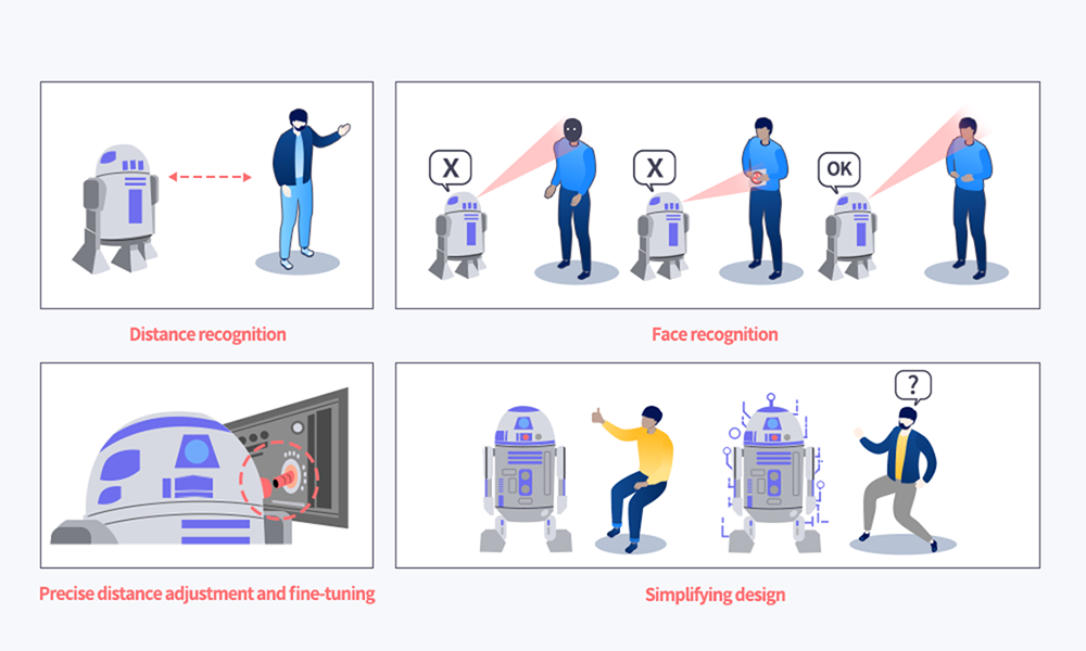
Fig 2. Necessary features of a machine’s eye
People can recognize objects multi-dimensionally and have depth perspective using two eyes and a brain. With a similar mechanism, machines too can recognize objects in multi-dimension and measure distance by applying a triangulation like stereo vision that uses two cameras and a processor. However, there are disadvantages such as complex calculation, lack of accuracy when it comes to measuring distance of a flat surface, and low accuracy in relatively darker places, which narrows the scope of application. Time-of-flight (ToF) has recently risen to the surface as an alternative to overcome these disadvantages. ToF is a simple method that measures the distance by the time light reflects off an object and returns. It is simple and fast to process. It also has the advantage of accurately measuring distance regardless of the luminous environment as it uses a separate light source.
ToF: To measure round-trip time of emitted light for acquiring the distance
Stereo Vision: Two optical systems observe the same target from two different points with respect to the same baseline

Fig 3. Comparison of how Stereo Vision and ToF recognize objects
Time-of-Flight
ToF can be categorized into direct ToF (d-ToF), which measures the distance based on the time light returns after being reflected off an object, and indirect ToF (i-ToF), which calculates the distance using the difference in phase shift of the returning light. SK hynix develops both ToF technologies so that they are utilized across various products. Who knows, maybe future robots will have one eye that uses i-ToF to recognize objects in close range, while the other eye uses d-ToF to explore the long distance.
This article aims to shed light on the i-ToF technology of SK hynix.

Fig 4. Comparative analysis of indirect ToF and direct ToF
The i-ToF method measures distance by calculating the phase difference from the light source by the proportion of electric charge accumulated in more than two different storages inside one pixel [1, 2]. With this mechanism, there is a limitation in measuring distance compared to d-ToF because there is less signal to isolate as light intensity weakens when it returns from a long distance. However, it has the advantage of delivering higher resolution compared to d-ToF because the circuit is simple making it easy to shrink pixels as pixels can isolate signals themselves. To make up for such limitation and maximize the advantage, there are a lot of studies being conducted on improving Signal to Noise Ratio (SNR), increasing QE of IR light source, or technology removing background light (BGL).
The current i-ToF pixel structure can be largely categorized into a gate structure and a diffusion structure. A gate structure is a method that collects surrounding electrons by applying modulated voltage4) to the photo gate to create an electric potential difference5) [2]. A diffusion structure collects electrons using the current generated by applying modulated voltage to the substrate as a current assisted photonic demodulator (CAPD) [3]. The latter can quickly detect electrons generated in deeper regions compared to the former, making transmission efficiency higher, but it requires more power consumption as it uses majority current [4]. In addition, it consumes even more power as pixels become smaller and the number of pixels increases to enhance resolution [5].
To maximize the advantages and minimize the limitations of CAPD, SK hynix developed a 10um QVGA6) grade and 5um VGA grade [6] pixel technology using a new structure called Vertical Field Modulator (VFM). Let’s take a deeper look into VFM technology and its strengths.
The Advantages of VFM Pixel Technology
There are various criteria that make a good distance measuring sensor, but first and foremost, it should accurately detect distance and have less heating issue by having lower power consumption. In other words, a good sensor must quickly detect signals at a higher efficiency with low power consumption, while it must also accurately separate signals according to phase shift.
1. SK hynix’s CIS Back Side Illumination Technology and Combination
Like CIS, there are a lot of advantages that back side illumination7) processing brings to the design or performance of ToF. The light source used to calculate the time of flight uses Infrared Ray (IR), because it must be invisible to the human eye. And it is used to calculate accurate distance even in low-light environment. Compared to visible light, IR has a longer wavelength meaning that most of the light is penetrated if a wafer thicker than that of CIS is not used, causing extremely low levels of signals generated in a pixel. But that doesn’t mean that the thickness can be extended infinitely. It is difficult to quickly collect electrons generated in deeper regions like how it is difficult to catch a fish in the deep sea compared to a fishing site. When applying back side illumination instead of front side illumination8), signal is quickly and easily detected as it creates a closer light collection where the electric field, which plays a role of the fishing line, is stronger by projecting light from the opposite side (Fig 5).
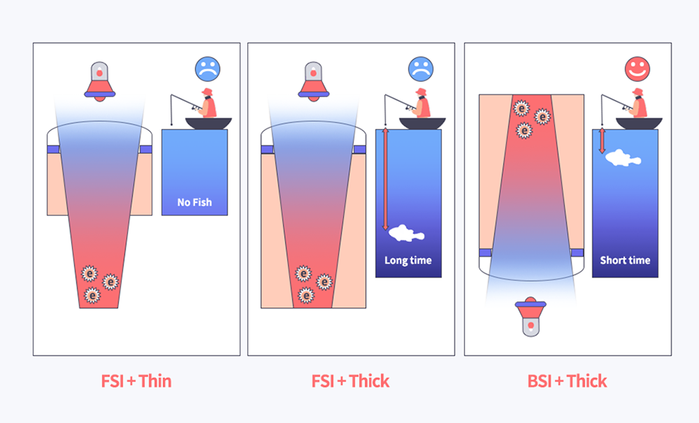
Fig 5. Comparison of FSI and BSI (Penetration ratio and light collection per thickness)
The performance of i-ToF depends on how well it isolates signals according to charge accumulation ratio. In this aspect, front side illuminated sensors may cause an error in distance because of a higher possibility that the light enters the detecting node neglecting phase difference in the process of passing through pixel surface. It is the same as doing a roll call and there is another student in the classroom. Also, back side illumination enables a wider option of metal routing which has many constraints to ensure higher fill factor9) in front side illumination, just like how it is more effective to draw water from underground rather than cutting down trees in a thick forest to collect rainwater (Fig 6).

Fig 6. i-ToF charge accumulation ratio according to method of illumination
(compared to drawing water from underground instead of cutting down trees in a thick forest)
This advantage can be realized by combining the CIS back side illumination technology of SK hynix, which has the technology to create pixels smaller than 1-micrometer (1/1000m).
2. SLA & Trench Guide Structure and Quantum Efficiency (QE)
According to the mechanism of i-ToF that uses charge accumulation ratio, maximum level of signal is required to obtain accurate distance data of an even greater distance. Therefore, high QE10) of the IR wavelength range11) is essential.
As explained above, the depth of light collection is deep due to the high penetration of IR light source, making light intensity weaker compared to visible light. There is a way of intentionally forming a micro lens structure (small-sized lenses arranged according to the size and number of pixels under a camera lens) high up to enable better light collection, but there is a limit to the height due to technical restrictions. SK hynix took a different approach to overcome the shortcoming. By placing several lenses smaller than the size of a pixel on each pixel, it increased light collection depth and thereby increased the total amount of light received.
SK hynix killed two birds with one stone by lengthening the transmission path of the light hitting the structure and returning by digging a special pattern in the back and making it focus onto the modulation region, thereby reducing light loss rate and increasing transmission efficiency with the same light intensity. In fact, this confirmed that QE more than doubled with 940nm light source. With higher QE, it successfully reduced the error between actual distance and measured distance by a whopping 55% compared to previous methods.
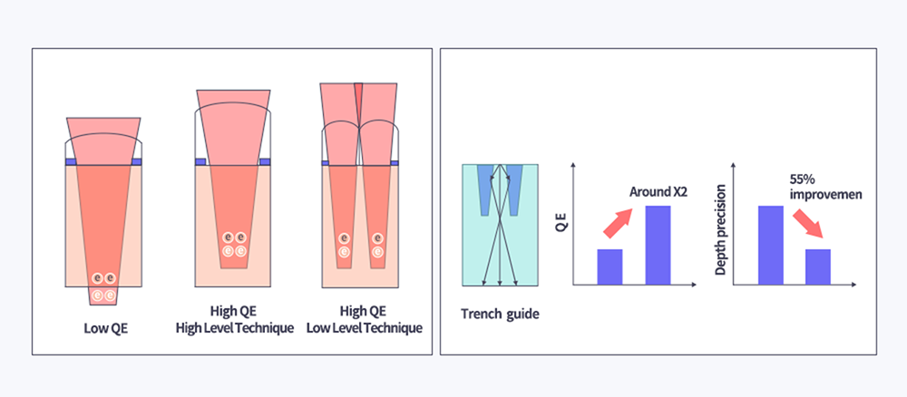
Fig 7. (Left/Right) SLA (Small Lens Array) / (Trench Guide)
3. Ensuring Low-Power, High-Performance
ToF sensors consume the most power in the circuit that modulates signals while in motion, excluding the power of the light source. The power of the modulation driver circuit is proportional to the electric current flowing across the circuit board. In other words, power consumption can be reduced by reducing substrate current. Also, accurate and precise distance measurement requires a short modulation cycle and fast signal detection. A vehicle (photon) has to speed up by hitting the accelerator in order to arrive at the same distance (Si thickness) quickly, which consumes that much fuel (or current). In another example, drawing up water from a deep well requires a lot of strength in lifting up the pulley. But what if you could draw up underground water with a pump? You could draw up as much water as you want without making an effort by simply turning on the faucet.
The VFM method increases the depletion region by optimizing the condition and structure of the pixel ion implantation to enable the pump-like role and strengthens the vertical electric field. As a result, the power of the electric field is added onto the current to effectively collect electrons, while also enabling fast collection even when the current is low, making it strong in terms of power consumption. Numerous experiments proved that the performance of VFM pixel depletes when the current increases, meaning that it is a structure more appropriate to low power and that current is no longer an important element. In other words, the method enhances pixel performance by securing a design that can realize a strong vertical electric field and controlling the current to simply play a guiding role. The 5um VGA-grade ToF sensor showed reduced current per pixel compared to a QVGA-grade ToF sensor even with smaller pixel size and higher resolution, showing almost zero increase in power consumption.

Fig 8. VFM with more efficient power consumption as ToF sensor
Summary
SK hynix develops ToF technology, while at the same time, contributes to generating economic and social value by enabling various module manufacturers to enter a vast range of application markets by offering close technology support and sensors.
We look forward to the depth solution technologies of SK hynix opening up a world where we travel around the world using AR/VR devices, a world where drones deliver packages and home droids bring them to us, a world where robot vacuum cleaners tidy up our homes as we watch the news in a self-driving car that opens by facial recognition.
Footnotes
1)CES: World’s largest technology show held in Las Vegas, U.S., as a venue for not only home appliances, but also new technologies for electronics across all industries including robotics and mobility.
2)Delivery robots: currently being operated as part of pilot programs by application companies or at some convenience stores.
3)AR: augmented reality, VR: virtual reality
4)Modulated voltage: voltage that switches pixel nodes to isolate signals.
5)Electric potential difference: energy difference across electrical positions in an electrical field. A charge moves from a low energy point to a high energy point.
6)QVGA: refers to a pixel’s resolution (320×240), VGA is 640×480
7)Back side illumination: a processing method that makes CIS in the order of ulens – color filter – PD – metal from top to bottom. The collection efficiency is much greater than using FSI + Light Guide.
8)Front side illumination: a processing method that makes CIS in the order of ulens – color filter – metal – PD from top to bottom.
9)Fill factor: the proportion of activated region (photodiode) out of the entire region of each pixel in a sensor.
10)QE: Quantum Efficiency, the measure of incident photons and converted electrons.
11)IR wavelength range: wavelength in the range of 750nm~1mm. ToF generally requires 850nm/940nm wavelength range.
References
[1]R. Lange, P. Seitz, A. Biber, and R. Schwarte, “Time-of-flight range imaging with a custom solid-state image sensor,” in Proc. SPIE, Laser Metrology and Inspection, Munich, Germany, 1999, vol. 3823.
[2]David Stoppa et al., “A Range Image Sensor Based on 10-um Lock-In Pixels in 0.18um CMOS Imaging Technology,” IEEE J. solid-state circuit, vol. 46, no. 1, pp. 248-258, Jan. 2011.
[3]Cyrus S. Bamji et al., “A 0.13um CMOS System-on-chip for a 512×424 Time-of-Flight Image Sensor With Multi-Frequency Photo-Demodulation up to 130MHz and 2GS/s ADC,” IEEE J. solid-state circuit, vol. 50, no. 1, pp. 303-319, Jan. 2015.
[4]Yuich Kato et al., “320×240 Back-Illuminated 10-um CAPD Pixels for High-Speed Modulation Time-of-Flight CMOS Image Sensor,” IEEE J. Solid-State Circuits, VOL. 53, NO. 4, pp1071-1078, Apr. 2018.
[5]L. Pancheri et al., “Current Assisted Photonic Mixing Devices Fabricated on High Resistivity Silicon,” SENSORS, IEEE, pp981-983, Oct. 2008.
[6]Y. Ebiko et al., “Low power consumption and high resolution 1280×960 Gate Assisted Photonic Demodulator pixel for indirect Time of flight,” 2020 IEEE International Electron Devices Meeting (IEDM), 2020, pp. 33.1.1-33.1.4.
[7]JH. Jang et al., “An Ultra-low current operating 5-μm Vertical Field Modulator Pixel for in-direct Time of Flight 3D Sensor.,” 2020 International Image Sensor Workshop (IISW), Sep. 2020.

ByJaehyung Jang
TL(Technical Leader) of CIS AR/VR Technology Project Team at SK hynix Inc.