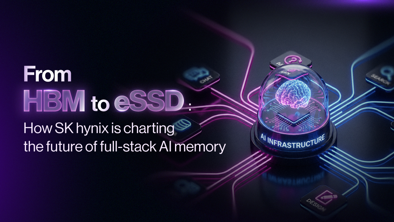
In his 1999 book, ‘Business @ the Speed of Thought,’ Bill Gates described a ‘Digital Nervous System’ as a connected world regardless of differences between time and space. As a requirement of this ‘Digital Nervous System,’ he stated how businesses should be operated at the speed of thoughts. This seemed impossible at that time, but seismic advancements have made this prediction possible in today’s world. The era of ultra-speed memory semiconductors has arrived.
TSV Technology: Unlocking HBM’s Unparalleled ‘Capacity and Speed’
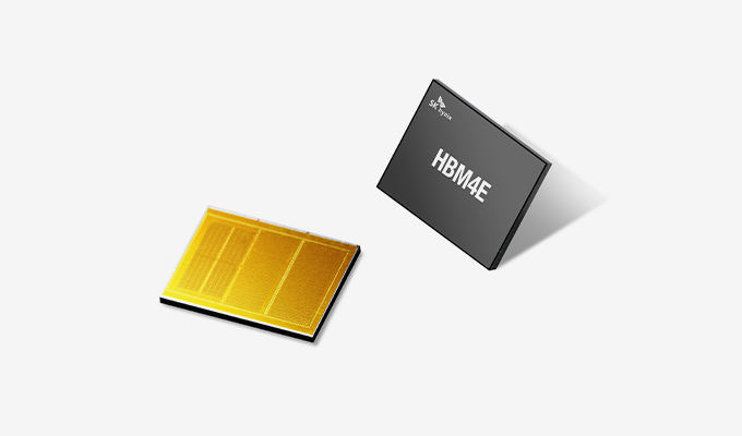
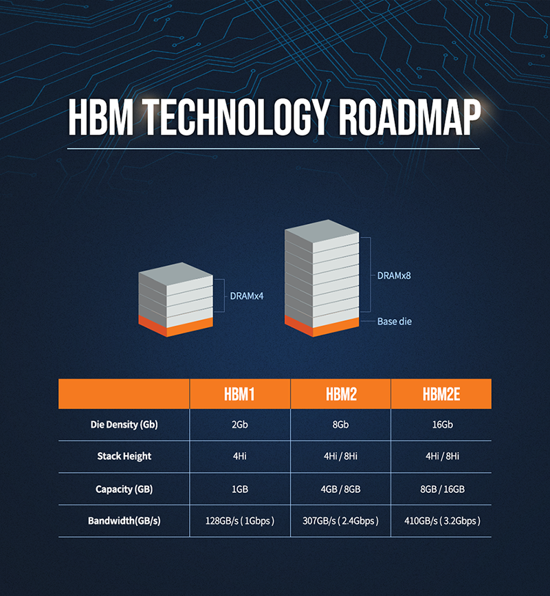
Semiconductor manufacturers have introduced High Bandwidth Memory (HBM) to increase data throughput and overcome the limits of bandwidth within a single package with through silicon via (TSV) technology for chip stacking. Along with this trend, SK hynix, which pioneered the development of HBM in 2013 in its strive for improved capacity and data transfer rates, realized its potential with its latest HBM2E, achieving 16GB by connecting eight 16Gb DRAM chips vertically through TSV.
TSV is composed of a circuit chip and multiple layers of DRAM on top of an ‘interposer,’ a functional package that sits between the circuit board and the chips. TSV is easier explained via a simple apartment building structure, where a community center (logic chip) is located above the building’s foundation (interposer), with each flat (DRAM) stacked up above. Unlike traditional methods, TSV technology drills numerous holes into chips and then stacks them one on top of the other. As a packaging technology, it connects chips through conductive electrodes inside these holes, which acts as a data elevator running through every layer from bottom to top that allows data to move vertically. This builds shorter connections than DRAM chips produced by traditional wire-bond connections, which results in a shorter signal path and a high-speed performance with lower power consumption. Moreover, penetrating the chip can create more passages between chips than traditional methods.

Evolution from HBM to HBM2E
HBM shows highly improved data processing rates when compared to DRAM packages that rely on wires. Unlike wire-bonding, HBM involves drilling over 5,000 holes into DRAM chips which are all connected to one another vertically with the help of TSV technology.
Based on this uprising industry trend, SK hynix developed an ultra-high-speed HBM2E in August 2019 that boasts the highest performance in the industry, making it the next-generation HBM DRAM product with its highly improved data processing rates – enhanced by 50% compared to previous HBM2 standards. While traditional structures package memory chips into a module form that can be connected to system boards, HBM chip is installed closely to logic chips, such as GPUs, with a gap of only dozens of µm units. This new structure creates shorter distances between chips, which accelerates data processing rates further.
Demand for high performance memory is expected to keep growing with the fourth industrial revolution, where the amount of data is exponentially increasing. HBM has already started to be adopted in GPUs. HBM2E is expected to be used as the high-end memory semiconductor for high-performance appliances that require ultra- high-speed characteristics, such as next generation GPUs, high-performance computing, cloud computing, and supercomputers, as well as playing an important role in technological sectors such as machine learning and AI- based systems. Also, for graphic application in the gaming industry, the adoption of HBM is largely increasing with the growing requirements to process more pixels for larger screens and provide higher computing rates for stable support of high-end gaming.