A New Attempt for the High-Speed
One day in 2008, the performance test for the graphic DRAM was in full swing at the Design Analysis Office at SK hynix (Hynix Semiconductor Inc. at that time). Joohwan Cho (DRAM PE), who was working hard on research, was the key person of the development and this is the person we will introduce in this article today.
“Graphic DRAM is a product specialized in ‘speed’, as it is optimal for fast data processing. If we could develop a high-speed technology for a graphic DRAM, it would mean that we could timely release higher performance products than our competitors, as it can be applied to main memory DRAMs or mobile DRAMs. At that time, SK hynix was also preparing a new graphic DRAM, GDDR5, with a goal of achieving 7Gbps speed (processing 7 gigabit of data per second). It can sound relatively slow when you compare it to the current level, but at that time, it was ‘SUPEX (Super Excellent)’, which means the highest level that humans can achieve, as a core concept of SK Group’s management. We set the high target like this from the beginning, as a ‘strategy’ to dominate the DRAM market.”
To achieve “7Gbps”, all existing designs had to be fundamentally changed. For this reason, the design team at that time attempted to apply the “2-Phase Clocking” design technology for the first time in the DRAM industry. “Clocking” is a method for synchronizing transmitted and received data during data transmission, and “2-Phase” is a technology that secures a spare time for operation by dividing the frequency. In other words, when comparing it to the water flow, this concept is like making the water flow in two pipelines and then combining two water flows afterwards, while the water flowed through only one pipeline previously.

In fact, Joohwan Cho had tried the “2-Phase Clocking” technology for the previous generation, GDDR4, but this did not lead to a great result. For him, GDDR4 meant the pain and a valuable lesson at the same time. Therefore, the success of GDDR5 was something he wanted to achieve and something he had to achieve. Also, as he took on the leader for this project at the relatively earlier stage of his career at that time, his sense of responsibility and his will was greater than anyone else.
The World’s first 40nm-class 2 Gigabit Graphic DDR5 Proves the “High Position” by Its Market Share
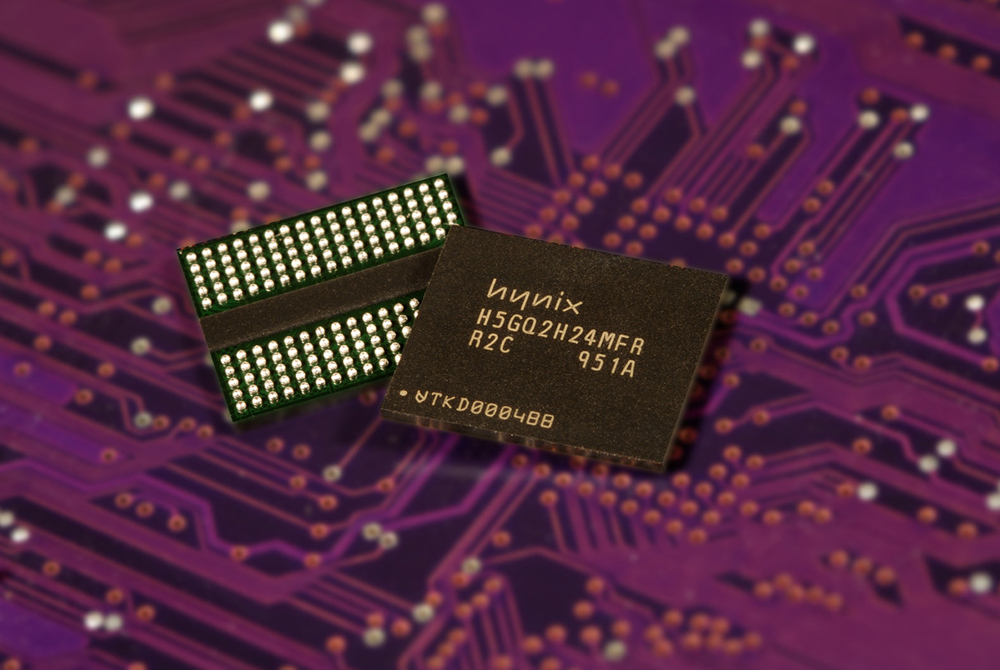
The product that was born after the enormous efforts was the 2 gigabit (Gb) GDDR5 where a 40nm-class process was applied for the first time in the world. This product could process 28 gigabytes (GB) of data per second through 32 input/output (I/O), with a processing speed of 7Gbps. The capacity was also doubled compared to the existing 50nm-class 1Gb product, which could meet the demand for high-capacity products. Also, energy consumption has been reduced by 20% compared to the previous one with low power operation of 1.35V.

40nm-class 2 gigabit (GB) graphic DDR5 product developed
by Hynix Semiconductor (predecessor to SK hynix)
Graphic DRAM was characterized by its capability of processing a large amount of data at once compared to general-purpose DRAM. GDDR5, which dramatically enhanced processing speed, was optimal for high-end desktops or laptops that required high-resolution and high-speed operation.
“Like today, early adopters, consumers who tend to purchase and use newly released products than others, used to measure the performance of newly released graphic cards by using various programs and share the results with others. There were many responses that SK hynix’s graphic DRAM was well ‘overclocked’. Here, overclocking means artificially controlling the chip performance to make it faster than it actually is. Consumer preference was very high in terms of performance as well. This suggests that this product was very competitive.”
Earlier, Hynix Semiconductor had succeeded in developing the world’s first 60nm-class 1Gb GDDR5 in 2007 and 50nm-class 1Gb GDDR5 in 2008, accounting for around 50% of the DRAM market’s share. With the development of the GDDR5 product, it secured a market share of nearly 70% and held an unchallenged position in the high-performance graphic DRAM market whilst leading the market.
Joohwan Cho, who has contributed to the development of SK hynix by committing himself to DRAM design for 27 years, has been recognized for his various achievements in Korea and other countries. The awards he has received so far include the In-house Year-end General Award, 38nm Graphic Special Award, and the SK Management System (SKMS) Practice Award. In 2015, he was recognized for his contribution to improving technological competitiveness by securing the 30nm-class GDDR5 design technology by receiving the Minister’s Award for the “Semiconductor Day” in Korea. As his career suggests, many products that have gone through his hands, but the 40nm-class 2Gb GDDR5 has always a special meaning to him.

“It was a product that made me realize and reminded me of the fact that we also have the DNA for taking the No.1 ranking and the ability to achieve it. The sense of accomplishment I felt at that time has been motivating me greatly even to this day. I believe that if we take the first place in several fields one by one, we will win the first place in the entire DRAM market. I hope the juniors also remember good precedents like GDDR5 and work with confidence.”


