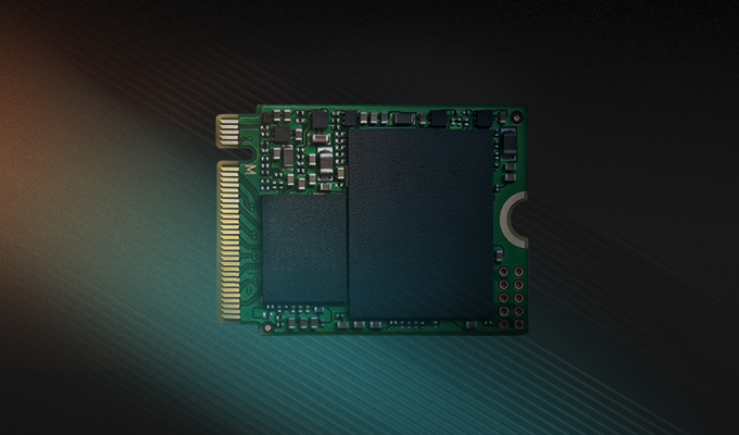
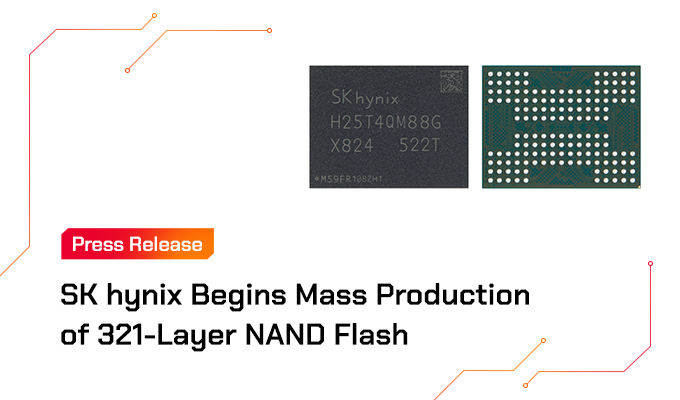
At the Flash Memory Summit (FMS) 2023 in August, SK hynix unveiled samples of the world’s first NAND flash memory with more than 300 layers. The 321-layer 1 Tb TLC 4D NAND was SK hynix’s another latest 4D NAND solution to break records since the company released its first 96-layer 4D NAND in 2018. These feats were made possible by the company’s 4D2.0 NAND technology, which improves on established technologies that reduce chip size and increase the number of layers while improving reliability and productivity.
This final episode in the Tech Pathfinder series will introduce SK hynix’s advanced 4D NAND technologies. These include its 4D1.0 technologies, which specialize in stacking and performance improvement such as the Cost-Effective 3-Plug formation, Sideway Source, All Peri.1 Under Cell (PUC), and Advanced Charge Trap Flash (CTF). It will also cover the 4D2.0 NAND technologies which overcome the limitations of stacking, such as Multi-Site Cell (MSC).
1Peripheral circuit (peri.): A circuit that controls the cell.
The Basics of NAND Flash Memory
For a better understanding of 4D NAND technology, it is prudent to review NAND’s basic concepts and related terminology.

Figure 1. An overview of different types of NAND flash memory
A cell is the smallest unit in which information is stored. In NAND flash memory, the cells consist of a control gate and a floating gate. When voltage is applied to the control gate, electrons traveling through the pathway are stored in the floating gate. NAND flash stores data by categorizing cells as either 0 or 1 using electrons stored on the floating gate. This state is characterized by the number of electrons in a cell. For example, a cell with few electrons is read as 0, while a cell with a high number of electrons is interpreted as 1.
NAND flash memory is categorized into different types depending on how much information (bits) is stored in a single cell. These include single-level cell (SLC, 1 bit), multi-level cell (MLC, 2 bits), triple-level cell (TLC, 3 bits), quad-level cell (QLC, 4 bits), and penta-level cell (PLC, 5 bits). As for the units used to measure NAND flash memory capacity, these include references to giga (a billion) and tera (a trillion). In other words, a TLC NAND flash product with a capacity of 1 Tb has about 330 billion cells that store 3 bits each.
4D1.0 Technology: Reducing Chip Size Through Cell Stacking
There are four main 4D1.0 NAND technologies SK hynix has employed to develop high-capacity NAND flash solutions.
Figure 2. An overview of the Cost-Effective 3-Plug formation and Sideway Source
Cost-Effective 3-Plug Formation
One of the key goals of developing semiconductor technology is improving cost efficiency. This is achieved by stacking more cells to reduce the chip size and producing as many chips as possible on a single wafer. Stacking substrates layer-by-layer and repeating the cell formation process for each layer would be inefficient and increase manufacturing costs. Therefore, multiple layers of substrate are first stacked, then vertical holes called plugs are drilled through the layers before cells are formed next to the holes.
As the number of layers increases, the more challenging it becomes to form plugs to the bottom layer as existing etching equipment can only etch around 100 layers at a time. Therefore, to develop a NAND flash product with more than 300 layers, it is necessary to stack 100 layers and perform the plug etching process three times. This is where SK hynix’s Cost-Effective 3-Plug formation is used as all the processes, including cell formation, can be performed simultaneously on all layers.
With this, SK hynix was able to conduct a single process to simultaneously fabricate the key structures—word lines2 and word line staircases3—that apply voltage and the passageways for electrons. This enabled the company to unveil a 321-layer 4D NAND of the highest density in August 2023 while minimizing costs.
2Word lines: The structure that binds the control gate of each layer of NAND cells.
3Word line staircases: A staircase-like structure for exposing the word line of each layer to the top surface.
Sideway Source
Semiconductor plugs provide a pathway for electrons to travel. Inside a plug, this pathway is covered by CTF film4. Therefore, the CTF film needs to be removed at the connection point where the plug and the bottom of the NAND flash layer meet to connect two pathways. Sideway source connects the plug to the bottom of the NAND flash layer (channel and source line5). Previously, etching gas was injected from the top of the plug to vertically remove the CTF film at the bottom of the plug. However, when stacking two or more plugs, the centers of the plugs were not aligned. This prevented the etching gas from reaching the bottom, damaging the CTF film on the side of the plug that serves as a cell.
4CTF film: A composite of oxide and nitride films that replaces the floating gate.
5Source line: Located at the bottom of a NAND layer, the source line is part of a channel inside the plug. Electrons from the source line travel up the channel to the top of the NAND layer and are stored in their respective floating gates.
SK hynix solved this issue by replacing the vertical connection with a horizontal one. The etching gas is injected into a separate pathway to reach the bottom of the NAND layer and remove the CTF film on both sides of the plug.
With Sideway Source technology, the etching gas is not directly injected into the plug. Therefore, even if the plugs are misaligned, the interior remains undamaged. As a result, SK hynix has significantly reduced its defect rate, increased productivity, and addressed the problem of increased costs associated with multiple stacking.
Since SK hynix introduced the industry’s first 4D NAND in 2018, it has enhanced its expertise to produce precise horizontal pathway connections which leave no voids at the bottom of the NAND layer. Based on this advancement, the company improved production efficiency by 34% for its 238-layer NAND flash memory compared to the 176-layer product and further solidified its market leadership with its 321-layer NAND.
Figure 3. An overview of All Peri. Under Cell (PUC)
All Peri. Under Cell (PUC)
PUC reduces the chip size and increases the number of stacks by placing the peripheral circuit (peri.) under the cell. SK hynix used PUC to develop a new NAND flash structure, the world’s first 4D NAND, and then began product development. The company has further developed upon PUC with its All PUC technology, which miniaturizes the peri. so it becomes the same size as the cell or smaller to accommodate the reduced cell size. To advance the technology, SK hynix is further miniaturizing the peri. by reducing the size and number of transistors and fully placing the peri. in the empty space under the cell.
In particular, this technology was used for the first time to great effect in SK hynix’s 238-layer 512 Gb TLC NAND. For this solution, the company reduced the size of the chip and peri. by more than 30% compared to the previous generation, thus improving production efficiency and cost competitiveness. SK hynix will continue to enhance its expertise and perfect the technology so it can be applied to future products that require a smaller peri. and chips.
Figure 4. An overview of Advanced Charge Trap Flash (CTF)
Advanced Charge Trap Flash (CTF)
Advanced CTF minimizes data degradation by retaining more electrons than conventional CTF. In CTF, electrons are stored in nonconductors rather than in conductors such as a floating gate. CTF was therefore developed in part to address inter-cell interference6 in conductors by changing the electron storage space to nonconductors. However, electrons often escape from nonconductors as they are stored in the voids of the CTF material (nitrogen-silicon compound) which has unstable areas. When electrons are stored in these unstable areas, the bonds quickly break and the electrons are ejected, resulting in data loss.
6Inter-cell interference: Electrons in a cell are affected by electrons in adjacent cells due to device miniaturization, resulting in data corruption.
For its Advanced CTF, SK hynix fills the unstable areas with hydrogen to prevent electrons from entering, and increases the number of binding agents to store more electrons. Furthermore, Advanced CTF also increases the number of electrons stored in CTF by minimizing the risk of escaped electrons. This improves the ability to determine electron counts, reduces read errors, and significantly shortens latency.
Some types of NAND flash have difficulties distinguishing data when there are a low number of electrons, resulting in errors. For example, if SLC flash memory distinguishes data using ten electrons, data with one to five electrons is 0, and data with six to ten electrons is 1. However, if five electrons escape, the data previously processed as 1 is distorted and an error occurs. This problem worsens as a cell is segmented to the MLC level and higher.
TLC differentiates between eight states from 000 to 111. If there are 10 electrons to distinguish, each state is assigned either one or two electrons. This is a significant difference from SLC, which allocates five electrons per state. Consequently, even if only a few electrons escape, it can lead to data corruption.
In contrast, consider a situation in which Advanced CTF was used to distinguish data with 100 electrons. If the number of electrons is between 0 and 50, the data is read as 0, while if it is between 51 and 100, it is 1. Even if some electrons escape, the large number of electrons overall greatly reduces the chance of misreading the data. Since there are few errors, the latency is shortened, and the read speed increases.
SK hynix first applied Advanced CTF to its 176-layer NAND solution, resulting in a 25% improvement in the ability to determine electron counts. As Advanced CTF-based memory solutions offer lower latency, they are particularly suited for the gaming and automotive markets which require rapid data processing.
4D2.0 Technology: Increasing Horizontal Cell Density & Stacking for Enhanced Performance & Density
When developing semiconductor memory, manufacturing costs continue to rise with each additional layer. Taking into account the additional cost of increasing the number of bits beyond the TLC level, there comes a point where it is no longer possible to reduce costs. In response, SK hynix is developing 4D2.0 technology which increases the number of layers and horizontal density of cells to improve storage capacity relative to cost. Multi-Site Cell (MSC) is a 4D2.0 technology that structurally improves the horizontal density, thereby significantly increasing the number of bits.
Figure 5. An overview of Multi-Site Cell (MSC)
Multi-Site Cell (MSC)
There are two primary methods for horizontally expanding cell density. The first is multi-level cell (MLC) technology, which subdivides electron counts to accommodate more data (bits) in a single cell. This is the case with NAND flash types ranging from SLC to QLC. The second is MSC technology, which structurally increases the sites where electrons are stored in a cell, enabling it to hold more data (bits).
MLC technology has been commercialized in 4-bit QLC products, but it is challenging to maintain performance and reliability in 5-bit PLC and beyond. This is due to the previously mentioned limitations in determining electron counts.
For example, if you build a 6-bit hexa-level cell (HLC) with MLC, you need to store data in 64 different states ranging from 000000 to 111111. This is prone to errors and time-consuming because there are not enough electrons to distinguish each state. Compared to the 4-bit QLC, the ability to determine the number of electrons is four times poorer.
On the other hand, when developing an HLC with MSC, eight states from 000 to 111 are created in two spaces and multiplied to realize 64 states to store data. Compared to the 4-bit QLC, the ability to distinguish electron counts doubles. In other words, it has the capacity of an HLC but the speed of a TLC. SK hynix has confirmed a 20-fold improvement7 in read and write speeds when utilizing MSC. Due to MSC’s high capacity, rapid speed, and reliability, SK hynix’s NAND flash is the leading solution for future multimodal AI8.
7Comparison between a 5-bit regular cell and a 2.5-bit × 2.5-bit MSC
8Multimodal AI: AI that can simultaneously process text, speech, images, etc.
Solving Industry Problems With An Eye on the Future
In this final Tech Pathfinder episode, SK hynix’s 4D NAND technologies were shown to solve the industry issues of today and tomorrow. The company’s 4D1.0 technologies improve the cost-effectiveness and performance of its NAND flash, while its 4D2.0 technologies will overcome stacking limitations set to arise in the future.
<Other articles from this series>
[Tech Pathfinder] HKMG Opens the Door to Leading Mobile DRAM LPDDR5X & LPDDR5T