Circuit-patterned wafers which have gone through a semiconductor fabrication (FAB) process are vulnerable to various factors including temperature changes, electric shocks, and chemical and physical external damage. To compensate for these weaknesses, chips are wrapped after separating them from the wafer. This method is known as “semiconductor packaging”. In common with semiconductor chips, packages also develop towards “light, thin, short and small”. At the same time, however, the packaging must not act as an obstacle when connecting signals from within the chips to outside the package. Packaging technology includes “internal structure technology”, “external structure technology”, and “surface mounting technology (SMT)”.
1. Package Development Flow
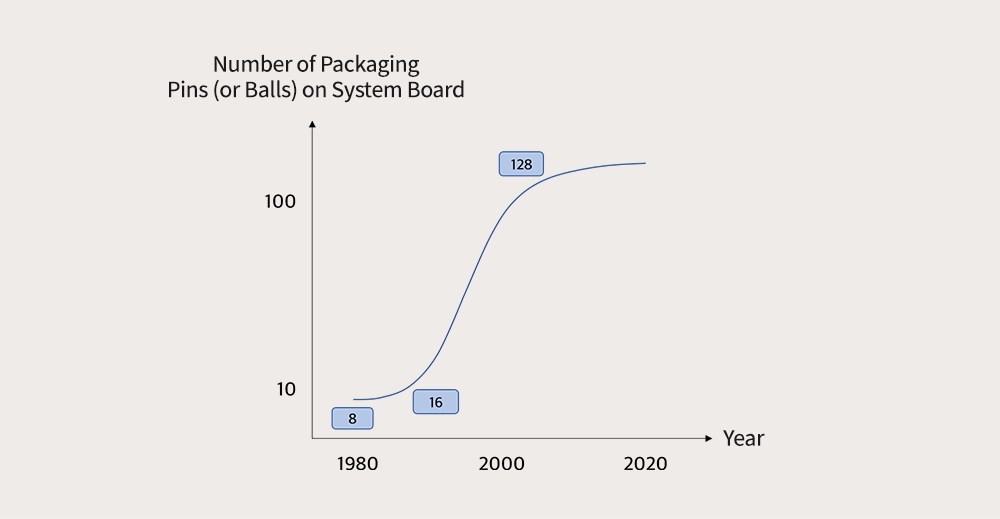
▲ Figure 1. Changes in the number of semiconductor packaging pins (or balls) in contact with the system board
To develop a new semiconductor package, the way of mounting the package on a system board and the external form of it must be changed. Then, the internal structure and material of the package must also be altered. When a package structure becomes complicated, the more the number of pins or balls in contact with the system board, the less the ball pitch – the distance between balls. The number of contact points between the package and the system board has rapidly approaching its limit and saturation point.
2. Package Structure
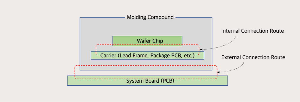
▲ Figure 2. Internal and external structure of semiconductor package
A semiconductor package’s structure consists of a semiconductor chip, a carrier (package PCB, lead frame, etc.) on which the chip is placed, and a molding compound which surrounds them.
In addition, the internal and external connection routes serve to connect signals from internal chips to the outside. Whether it be an internal or external connection, this connection was previously made with lines (wires or lead frames). Recently, however, points (bumpers or balls) are typically being used. Meanwhile, molding compounds play an important role in taking out the heat inside and protecting the chip from external damage.
3. Three Elements Determining Package Types: Internal Structure, External Structure and Mounting
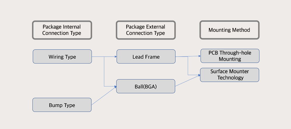
▲ Figure 3. Diagram of package internal connection type, external connection type and mounting method
Until the late 1980s, the mainstream package internal connection type was the wire bonding method, which connects the pad on the chip to the pad on the carrier with gold wires. However, as package sizes decreased, the volume occupied by the metal wires within the package increased with it. To solve this problem, instead of removing the metal wires, bumps were used to replace them for internal connections. Of course, that does not mean the wire bonding method became completely unavailable. When bumps are used, it requires the bump attaching process and epoxy under-fill methods instead of the die-attaching and wire bonding processes.
The external connection type has also shifted from the use of lead frames to balls. This is because lead frames have the same disadvantages as wires. While the “wire – lead frame – PCB through-hole mounting” was used before, now the method of “bump – ball grid array (BGA) – surface mounter technology” is the most commonly utilized.
4. Internal Package Type
4.1 Wireless Semiconductor, Flip Chip
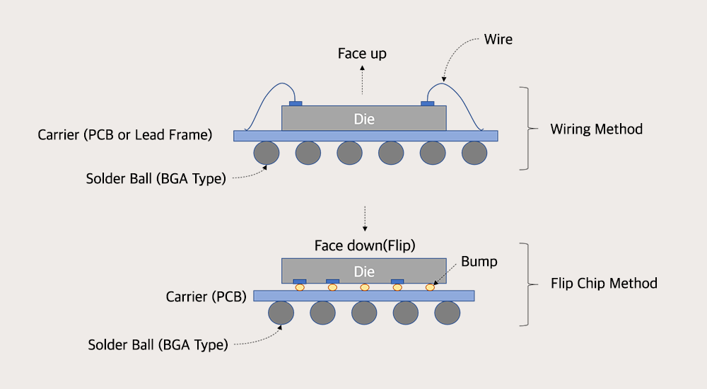
▲ Figure 4. Comparison of wire bonding type and flip chip type
Semiconductor packages can be classified according to internal structure: wiring and flip chip. The wiring method connects the chip and the carrier through wire bonding, with a face up. On the other hand, the flip chip method involves very small diameter balls (a conductive metal called “bump”) being connected to the pad with a face down. In other words, with the flip chip method, the semiconductor chip is in contact with the board without the use of long wires. For this reason, it features a shorter signal travel distance and a more powerful adhesion strength. It is a groundbreaking method in that it addresses the various problems usually associated with wiring.
The greatest advantages of the flip chips are that they reduce the volume of the package and improve the power consumption and signal flow. Due to its shorter length, there are less effect of electrical resistance and noise from the surrounding area, making it faster. Also, what kind of metal a bump is important. Currently, solder or gold is typically used. Deciding what kind of epoxy material to fill the gap between bumps and carrier is another important matter. Besides, since it doesn’t use wires that occupy a large area, the size of the chip after molding can be reduced. This is why it is widely used in small electronic devices like mobile phones. That is, as the footprint area of the package on the system board is reduced, it is applied to high-density board technology. This means a major transformation in the packaging method, with the advent of miniaturized electronic devices such as smartphones.
4.2 TSV (Through Silicon Via), 3D Package Made by Draining Holes in Chips
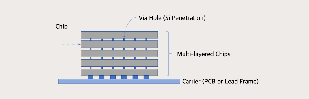
▲ Figure 5. 3D Package with Via Hole penetrating silicon chips
We utilize a multi-layered packaging that stacks multiple semiconductor chips to increase the density of the chip package. Multi-chip packaging at the wafer level includes the wire bonding method and Through Silicon Via (TSV). In TSV, once chips are stacked, then you drain holes through them vertically to connect signal lines by using silicon through electrodes. Through this method, the speed of signals is faster and the density of the package can be higher. If the existing method of handling one single chip is regarded as 2D packaging, TSV can be considered 3D packaging. If multi-layered chips are connected with wires, a step-stack structure is formed, increasing the area by about two times. However, in TSV, a direct-stack structure is formed like an apartment building, requiring only around 1.2 times the chip area. TSV, which has excellent area efficiency, is now expanding its application to other fields.
5. External Package Type and Mounting Methods @Based on How the Package Connects to the Outside
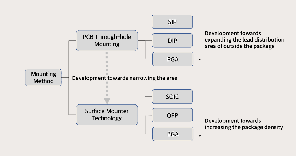
▲ Figure 6. Types of external package type and mounting methods
5.1 External Package Type
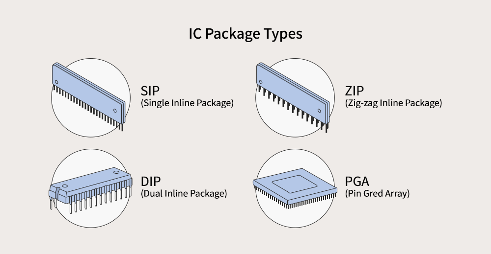
▲ Figure 7. IC Package Types
There are numerous types of packaging chips. As a lead frame type, there is a dipping type suitable for PCB through-hole mounting, which has been developed in the order of SIP1, ZIP2, DIP3, and PGA4. However, since its ability to reduce the footprint area occupying the system board is limited, it is currently used only in some cases.
Meanwhile, among the lead frame types, small outline (SO) is one of surface mounter technologies where the lead is bent to increase the integration. It has been developed to SOIC and SOJ (J type) and is still used widely. In addition to this, a quad flat package (QFP) where the bent leads are applied on four edges is used in CPU chips. After that, the package changed dramatically from the lead frame type to the ball type, presenting a BGA. These days, the ball type is in the more mainstream system.
5.2 Mounting Methods
The package mounting methods are largely divided into surface mounter technology (SMT) and PCB through hole. As the name suggests, SMT fixes a chip to the system board surface via soldering. PCB through hole is a method of cutting a chip’s lead pins into a hole on the system board and then fixing it with soldering
In this method, however, the area occupied by holes on the system board was too large. For light, thin, short, and small packages, the mounting method has also been developed into a surface mounter technology without holes. Among the lead frame methods, SO type (SOIC and SOJ) and TSOP have been developed for surface mounting from the beginning. For the BGA type, it also applies the surface mounting method as well because the ball itself is for mounting on the system board.
Packages have been developing towards “light, thin, short and small packages”. To achieve this, the internal and external shape of the package and mounting methods are changing at the same time. In terms of power, speed, and environment, semiconductor package chips require a high level of performance. They are also transforming in terms of materials to satisfy this. The priority that packages change is usually structure, material, and function in order, but this doesn’t apply to all cases. Package types can be classified as follows: MCP (Multi Chip Package), SiP (System in Package), PoP (Package on Package), CSP (Chip Scale Package), and so on. On this wise, package types can be classified in various ways according to different perspectives. To avoid the confusion that can be caused by this, the structure of the packaged products has become the basis for classification in this chapter.
* SIP (Single Inline Package): SIP is a package where the pins are arranged in a single row.
* ZIP (Zig-zag Inline Package): ZIP is a package where the pins are arranged in a zig-zag form.
* DIP (Dual Inline Package): DIP is a package where the pins are arranged in two rows.
* PGA (Pin Grid Array): PGA is a package with the square or rectangular shape, in which the pins are arranged in a regular array on the underside of the package.

By Jong-moon Jin
Teacher at Chungbuk Semiconductor High School